Digital Principles and Computer Organization: Unit II (a): Synchronous Sequential Logic
Two marks Questions with Answers
Synchronous Sequential Logic - Digital Principles and Computer Organization
In a level triggered J-K flip-flop, when J and K are both high, then the output toggles continuously. This condition is called a race around condition.
Two Marks Questions with
Answers
Q.1 Give the excitation table of SR flip-flop.
(Refer section 2.5.3.1)AU: Dec.-03
• Table 2.5.2 (a) and (b)show the truth table and excitation tables for SR flip-flop, respectively.
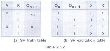
• There are four possible transitions from the present state to the next state.
• For each transition, the required input condition is derived from the information available in the truth table.
Note The symbol "X" in the table represents a don't care condition, i.e., it indicates
that to get required output it does not matter whether the input is either 1 or 0.
• 0 → 0 Transition: The present state of the flip-flop is 0 and is to remain 0 when a clock pulse is applied. Looking at truth table of SR flip-flop we can understand that, this can happen either when R = S = 0 (no-change condition) or when R = 1 and S = 0. Thus, S has to be at 0, but R can be at either level. The table indicates this with a "0" under S and an "X" (don't care) under R.
• 0 → 1 Transition: The present state is 0 and is to change to 1. This can happen only when S = 1 and R = 0 (set condition). Therefore, S has to be 1 and R has to be 0 for this transition to occur.
•1→ 0 Transition: The present state is 1 and is to change to a 0. This can happen only when S = 0 and R = 1 (reset condition). Therefore, S has to be 0 and R has to be 1 for this transition to occur.
• 1 → 1 Transition: The present state is 1 and is to remain 1. This can happen either when S = 1 and R = 0 (set condition) or when S = 0 and R = 0 (no change condition). Thus R has to be 0, but S can be at either level. The table indicates this with a "X" under S and "0" under R.
Ans. :In a level
triggered J-K flip-flop, when J and K are both high, then the output toggles
continuously. This condition is called a race around condition.
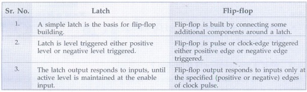
Q.3 Differentiate between flip-flop and
latch. AU
May-05, 19
Ans. :
Q.4 Give the excitation table for JK flip-flop.
(Refer section 2.5.3.2) AU : May-05, 09• The truth table and excitation table for JK flip-flop are shown in Table 2.5.3 (a) and (b) respectively.
• 0 → 0 Transition: When both present state and next state are 0, the J input must remain at and the K input can be either 0 and 1.
• 0 → 1 Transition: The present state is 0 and is to change to 1. This can happen either when J = 1 and K = 0 (set condition) or when J = K = 1 (toggle condition). Thus, J has to be 1, but K can be at either level for this transition to occur.
• 1 → 0 Transition: The present state is 1 and is to change to 0. This can happen either when J = 0 and K = 1 or when J = K = 1. Thus, K has to be 1 but J can be at either level.
• 1→ 1 Transition: When both present state and next are 1, the K input must remain at 0 while the J input can be 0 or 1.
• The excitation table for JK flip-flop has more don't care conditions than the excitation table for RS flip-flop.
• The don't care terms usually simplify the function. Therefore, the combinational circuits using JK flip-flops for the input functions are likely to be simpler than those using RS flip-flops.
(Refer sections 2.5.3.3 and 2.5.3.2) AU:
May-06
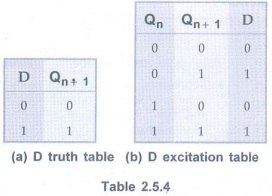
D Flip-Flop
• The Table 2.5.4 (a) and (b) show the truth table and excitation table for
D flip-flop, respectively.
• In D flip-flop, the next state is always equal to the D input and it is independent of the present state. Therefore, D must be 0 if Qn+1 has to be 0, and 1 if Qn+1 has to be 1, regardless of the value of Qn.
JK Flip-Flop
• The truth table and excitation table for JK flip-flop are shown in Table 2.5.3 (a) and (b) respectively.
• 0→0 Transition: When both present state and next state are 0, the J input must remain at and the K input can be either 0 and 1.
• 0 → 1 Transition: The present state is 0 and is to change to 1. This can happen either when J = 1 and K = 0 (set condition) or when J = K = 1 (toggle condition). Thus, J has to be 1, but K can be at either level for this transition to occur.
• 1→0 Transition: The present state is 1 and is to change to 0. This can happen either when J = 0 and K = 1 or when J = K = 1. Thus, K has to be 1 but J can be at either level.
• 1→ 1 Transition: When both present state and next are 1, the K input must remain at 0 while the J input can be 0 or 1.
• The excitation table for JK flip-flop has more don't care conditions than the excitation table for RS flip-flop.
• The don't care terms usually simplify the function. Therefore, the combinational circuits using JK flip-flops for the input functions are likely to be simpler than those using RS flip-flops.
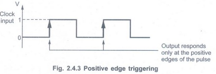
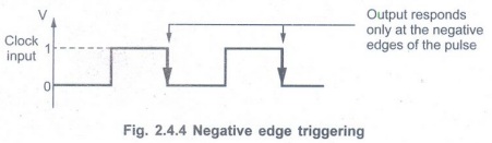
Q.6 Give the meaning for edge triggering in flip-flops. AU: Dec.-06, 07, May-17, 19
Ans.: In the edge
triggering, the output responds to the changes in the input only at the positive
or negative edge of the clock pulse at the clock input. There are two types of
edge triggering.
• Positive edge triggering: Here,
the output responds to the changes in the
input only at the positive edge of the
clock pulse at the clock input.
• Negative edge triggering: Here,
the output responds to the changes in the input only at the negative edge of
the clock pulse at the clock input.
Q.7 If the input frequency of a T FF is
1600 kHz, what will be the output frequency? Give reason for your answer. AU: Dec.-06
Ans. :800 kHz, because
it toggles at every clock pulse.
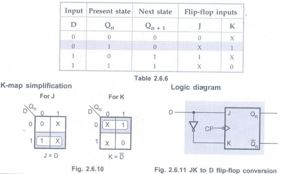
Q.8 Convert JK FF to D FF.
(Refer section 2.6.5) AU : May-07
• The excitation table for above conversion is as shown in the Table 2.6.6.
Q.9 Define a sequential logic circuit.
Give an example. AU: May-08
Ans. : The circuits in
which the output variables depend not only on the present input but they also
depend upon the past history of these input variables are known as sequential
logic circuits. Flip-flops, counters, registers are the examples of sequential
logic circuit.
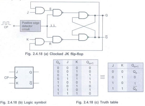
Q.10 Draw the logic circuit of a clocked JK flip-flop.
(Refer section 2.4.5) AU: May-08
Q.11 Differentiate between combinational
and sequential circuits.
(Refer section 2.1.1) AU: May-03, 05,
10, Dec.-02, 03, 04, 07, 08, 09

Q.12 What are synchronous sequential
circuits ?AU: May-10
Ans. :Synchronous
sequential circuits are those in which signals can affect the memory elements
only at discrete instants of time. Clocked flip-flops are examples of
synchronous sequential circuits.
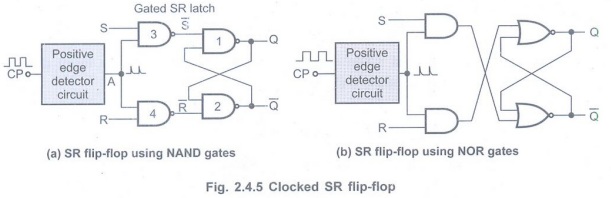
Q.13 Draw the circuit of SR flip-flop.
(Refer section 2.4.3) AU: May-10
Q.14 Give the characteristic equation and state diagram of JK flip-flop. AU: May-07, 10, June-13
Ans. :
Q.15 What is the operation of D flip-flop
?
Ans. : In D flip-flop
during the occurrence of clock pulse if D = 1, the output Q is set and if D =
0, the output is reset.
Q.16 What is the operation of JK
flip-flop ?AU: Dec.-16
Ans. :
• When K input is low and J input is high
the Q output of flip-flop is set.
• When K input is high and J input is low
the Q output of flip-flop is reset.
• When both the inputs K and J are low
the output does not change.
• When both the inputs K and J are high
the output toggle on the next positive clock edge.
Q.17 What is the operation of T flip-flop
?
Ans. : T flip-flop is
also known as Toggle flip-flop.
• When T = 0 there is no change in the
output.
• When T = 1 the output switch to the
complement state (i.e.) the output toggles.
Q.18 What is a master-slave flip-flop ?
Ans. : A master-slave
flip-flop consists of two flip-flops where one circuit serves as a master and
the other as a slave. The output of the master flip-flop is fed as an input to
the slave flip-flop. The master flip-flop is triggered at the positive edge of
the clock and slave flip-flop is triggered at the negative edge of the clock.
Q.19 Derive the characteristic equation of a D flip-flop.
(Refer section 2.5.1) AU: Dec.-02
Q.20 What are the various types of triggering of FFs ?
(Refer section 2.4.2) AU: Dec.-03
Level Triggering
• In the level triggering, the output state is allowed to change according to input(s) when active level (either positive or negative) is maintained at the enable input.
Edge Triggering
•In the edge triggering, the output responds to the changes in the input only at the positive or negative edge of the clock pulse at the clock input.
Q.21 Derive the characteristic equation of a T flip-flop.
(Refer section 2.5.1) AU: May-04
Q.22 Derive the characteristic equation of a SR flip-flop.
(Refer section 2.5.1) AU: Dec.-02
Q.23 Derive the characteristic equation of a JK flip-flop.
(Refer section 2.5.1) AU: May-03, 14
Q.24 How will you convert a JK flip-flop into a D flip-flop ?
(Refer section 2.6.5) AU: Dec.-03
• The excitation table for above conversion is as shown in the Table 2.6.6.
Q.25 What is meant by the term 'edge
triggered'?
(Refer section 2.4.2) AU: May-04
•In the edge triggering, the output responds to the changes in the input only at the positive or negative edge of the clock pulse at the clock input.
• There are two types of edge triggering.
• Positive edge triggering: Here, the output responds to the changes in the input only at the positive edge of the clock pulse at the clock input.
• Negative edge triggering: Here, the output responds to the changes in the input only at the negative edge of the clock pulse at the clock input.
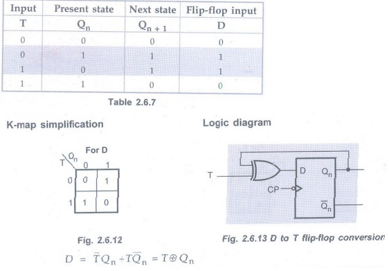
Q.26 How can a D flip-flop be converted
into a T flip-flop ?
(Refer section 2.6.6) AU: Dec.-05,
May-07
The excitation table for above conversion is as shown in the Table 2.6.7.
Q.27 Draw the internal circuit of a NOR gate latch and derive the truth table.
(Refer section 2.2) AU:
May-06

• The basic bistable element circuit has two stable states logic 0 and logic 1, hence the name 'bistable'.
• When A = 0, the output of inverter 1 is 1 (A), i.e., Q = 1
• Since the output of the inverter 1 is connected to the input of the inverter 2, Ā = B = 1. Consequently, the output of inverter 2, i.e., ![]() is 0.
is 0.
• Since the output of the inverter 2 is connected to the input of the inverter 1, ![]() =
= ![]() = A = 0.
= A = 0.
• We have assumed same value for A. Thus, the circuit is stable with = A = ![]() = 0 and Q = Ā = B = 1.
= 0 and Q = Ā = B = 1.
• Using similar explanation it is easy to show that if it is assumed that A = 1 basic bistable element is stable with ![]() = A =
= A = ![]() = 1 and Q= Ā = B = 0. This is a second stable condition of the basic bistable element.
= 1 and Q= Ā = B = 0. This is a second stable condition of the basic bistable element.
(Refer section
2.5.2) AU: May-06
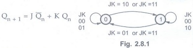
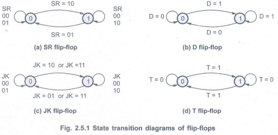
• Fig. 2.5.1 shows the state transition diagram for all flip-flops. Here, the 0 and the 1 in the circle represents the two states of the flip-flops and the arcs with arrow heads indicate the state transitions for specific inputs of the flip-flop.
• For example, when SR flip-flop is in state 0, it goes to state 1 if SR inputs are 10, i.e. S = 1 and R = 0.
Q.29 Draw the diagram of a clocked SR flip-flop using four NAND gates.
(Refer section 2.4.3) AU:
Dec.-04
Q.30 Draw the logic diagram for D-type latch.
(Refer section 2.3.2) AU: Dec.-07
Q.31 Draw the logic diagram for T flip-flip. (Refer section 2.4.9)
Q.32 Write down characteristics table of JK
flip-flop.
(Refer section 2.4.5) AU: May-08
Case 1 : J = K = 0
When J = K = 0, S = R = 0 and according to truth table of SR flip-flop there is no change in the output.
When inputs J = K = 0, output does not change.
Case 2: J= 1 and K = 0
Q = 0, ![]() =1: When J=1,K=0 and Q=0,S=1 and R=0.According to truth table of SR flip-flop it is set state and the output Q will be 1.
=1: When J=1,K=0 and Q=0,S=1 and R=0.According to truth table of SR flip-flop it is set state and the output Q will be 1.
Q = 1, ![]() =0: When J = 1, K = 0 and Q = 1, S = 0 and R = 0. Since SR = 00, there is no change in the output and therefore, Q = 1 and
=0: When J = 1, K = 0 and Q = 1, S = 0 and R = 0. Since SR = 00, there is no change in the output and therefore, Q = 1 and ![]() = 0.
= 0.
The inputs J = 1 and K = 0, makes Q = 1, i.e. set state.
Case 3: J= 0 and K = 1
Q = 0, ![]() = 1: When J = 0, K = 1 and Q = 0, S = 0 and R = 0. Since SR there is no change in the output and therefore, Q = 0 and
= 1: When J = 0, K = 1 and Q = 0, S = 0 and R = 0. Since SR there is no change in the output and therefore, Q = 0 and ![]() = 1.
= 1.
Q = 1, ![]() = 0: When J 0, K = 1 and Q = 1, S = O and R = 1. According to truth table of SR flip-flop it is a reset state and the output Q will be 0.
= 0: When J 0, K = 1 and Q = 1, S = O and R = 1. According to truth table of SR flip-flop it is a reset state and the output Q will be 0.
The inputs J = 0 and K = 1, makes Q = 0, i.e., reset state.
Case 4: J = K = 1
Q = 0, ![]() = 1: When J = K = 1 and Q = 0, S = 1 and R=0.According to truth table of SR flip-flop it is a set state and the output Q will be 1.
= 1: When J = K = 1 and Q = 0, S = 1 and R=0.According to truth table of SR flip-flop it is a set state and the output Q will be 1.
Q = 1, ![]() = 0: When J = K = 1 and Q = 1, S = 0 and R = 1. According to truth table of SR flip-flop it is a reset state and the output Q will be 0.
= 0: When J = K = 1 and Q = 1, S = 0 and R = 1. According to truth table of SR flip-flop it is a reset state and the output Q will be 0.
The input J = K = 1, toggles the flip-flop output.
(Refer section 2.7.1) AU: Dec.-08, May-12, 14. AU: Dec.-08
• Reading taken during bouncing period may be faulty. This problem is known as key debounce.
• The problem of key debounce is undesirable and it must be avoided.
• One way to avoid key debounce problem is to use SR latch.
• The circuit used to avoid keybounce with SR latch is called a switch or contact debouncer.
• When key is at position A, the output of SR latch is logic 1 and when key is at position B, the output of SR latch is logic 0.
• When key is in between A and B, SR inputs are 00 and hence output does not change, preventing debouncing of key output.
• We can say that the output does not change during transition period, eliminating key debounce.
Q.34 What is race around condition?
(Refer section 2.4.5.2) AU: Dec.-09, May-14
• In JK flip-flop, when J = K = 1, the output toggles (output changes either from 0 to 1 or from 1 to 0).
• Consider that initially Q = 0 and J = K = 1. After a time interval At equal to the propagation delay through two NAND gates in series, the output will change to Q = 1 and after another time interval of At the output will change back to Q=0. This toggling will continue until the flip-flop is enabled and J = K = 1. At the end of clock pulse the flip-flop is disabled and the value of Q is uncertain. This situation is referred to as the race-around condition. This is illustrated in Fig. 2.4.22.
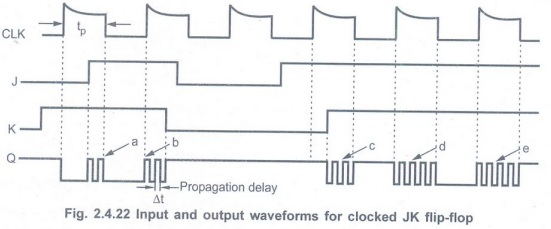
This condition exists when tp ≥ ∆t. Thus by keepingtp ≥ ∆t we can avoid race
around condition.
• We can keep tp ≥ ∆t by keeping the duration of edge less than ∆t.
• A more practical method for overcoming this difficulty is the use of the Master-Slave (MS) configuration.
Q.35 Differentiate flip-flop from latches.
(Refer section 2.4.1) AU: May-10
• Latches and flip-flops are the basic building blocks of the most sequential circuits.
• The main difference between latches and flip-flops is in the method used for changing their state.
• A simple latch forms the basis for the flip-flop.
• Latches are controlled by enable signal, and they are level triggered, either positive level triggered or negative level triggered.
• The output state is free to change according to the S and R input values, when active level is maintained at the enable input.
• Flip-flops are pulse or clock edge triggered instead of level triggered
Q.36 Draw the excitation table and state
diagram for JK and SR flip-flop.
(Refer sections 2.5.3.2 and 2.5.3.1) AU
: May-10
Q.37 Write the state transition table of J-K flip-flop.
(Refer section 2.5.3.2) AU: May-11
• 0→0 Transition: When both present state and next state are 0, the J input must remain at and the K input can be either 0 and 1.
• 0 → 1 Transition: The present state is 0 and is to change to 1. This can happen either when J = 1 and K = 0 (set condition) or when J = K = 1 (toggle condition). Thus, J has to be 1, but K can be at either level for this transition to occur.
• 1→0 Transition: The present state is 1 and is to change to 0. This can happen either when J = 0 and K = 1 or when J = K = 1. Thus, K has to be 1 but J can be at either level.
• 1→ 1 Transition: When both present state and next are 1, the K input must remain at 0 while the J input can be 0 or 1.
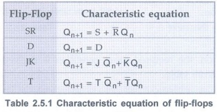
Q.38 Express the next state characteristics of D and SR flip-flops. AU: May-11
Ans. : For D flip-flop : Qn+1
Qn+1 = S + Ȓ Qn
Q.39 List any two mechanisms to achieve edge triggering of flip-flops. AU: Dec.-12
Ans. : 1. Positive
edge triggering 2. Negative edge triggering.
Q.40 With reference to a JK flip flop, what is racing?
(Refer section 2.4.5.2) AU: Dec.-14
• In JK flip-flop, when J = K = 1, the output toggles (output changes either from 0 to 1 or from 1 to 0).
• Consider that initially Q = 0 and J = K = 1. After a time interval At equal to the propagation delay through two NAND gates in series, the output will change to Q = 1 and after another time interval of At the output will change back to Q=0. This toggling will continue until the flip-flop is enabled and J = K = 1. At the end of clock pulse the flip-flop is disabled and the value of Q is uncertain. This situation is referred to as the race-around condition.
Q.41 Give the block diagram of Maser-Slave D flip-flop.
(Refer section 2.4.7) AU: May-15
It consists of clocked D flip-flop as a master and another clocked D flip-flop as a slave.
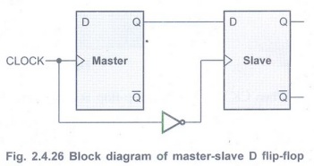
• Both the flip-flops are positive level triggered, but inverter connected at the clock input of the slave flip-flop forces it to trigger at the negative level.
• D input is transferred to the master at the positive edge of the clock pulse and the same is copied by the slave and therefore appears at the output Q of the slave flip-flop at the negative going edge of the clock pulse.
Q.42 State the operation of T flip-flop.
(Refer section 2.4.9) AU: Dec.-18
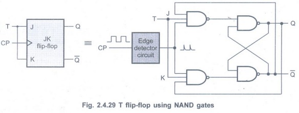
• T flip-flop is also known as 'Toggle flip-flop'.
• The T flip-flop is a modification of the JK flip-flop.
• As shown in the Fig. 2.4.29, the T flip-flop is obtained from a JK flip-flop by connecting both inputs, J and K together.
• When T = 0, J = K = 0 and hence there is no change in the output. When T = 1, J = K = 1 and hence output toggles.
Q.43 What is race around condition?
(Refer section 2.4.5.2) AU: Dec.-18
• In JK flip-flop, when J = K = 1, the output toggles (output changes either from 0 to 1 or from 1 to 0).
• Consider that initially Q = 0 and J = K = 1. After a time interval At equal to the propagation delay through two NAND gates in series, the output will change to Q = 1 and after another time interval of At the output will change back to Q=0. This toggling will continue until the flip-flop is enabled and J = K = 1. At the end of clock pulse the flip-flop is disabled and the value of Q is uncertain. This situation is referred to as the race-around condition. This is illustrated in Fig. 2.4.22.
This condition exists when tp ≥ ∆t. Thus by keepingtp ≥ ∆t we can avoid race
around condition.
• We can keep tp ≥ ∆t by keeping the duration of edge less than ∆t.
• A more practical method for overcoming this difficulty is the use of the Master-Slave (MS) configuration.
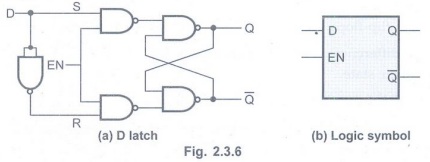
(Refer section 2.4.3) AU: May-19
• The NAND gates 1, 2, 3 and 4 form the basic SR latch with enable input.
• The fifth NAND gate is used to provide the complemented inputs.
• As shown in the Fig. 2.3.6, D input goes directly to the S input and its complement is applied to the R input, through gate 5. Therefore, only two input conditions exists, either S = 0 and R = 1 or S = 1 and R = 0.
• The truth table for D latch is as shown in the Table 2.3.2.
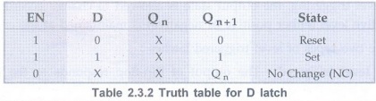
• As shown in the truth table, the Q output follows the D input. For this reason D latch is sometimes called transparent latch.
Digital Principles and Computer Organization: Unit II (a): Synchronous Sequential Logic : Tag: : Synchronous Sequential Logic - Digital Principles and Computer Organization - Two marks Questions with Answers
Related Topics
Related Subjects

Digital Principles and Computer Organization
CS3351 3rd Semester CSE Dept | 2021 Regulation | 3rd Semester CSE Dept 2021 Regulation