Digital Principles and Computer Organization: Unit I: Combinational Logic
Two marks Questions with Answers
Combinational Logic - Digital Principles and Computer Organization
Representing the minterms of the sum of product expression in the Karnaugh-map of appropriate variables is known as variable mapping.
Two Marks Questions with
Answers
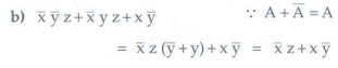
Q.1 Show that
a) a + a'b = a + b) x'y' z + x'yz + xy'
= x'z + xy'. AU: May-10
Ans.: a) Refer section
2.4.2.
Q.2 What is variable mapping? AU:
May-07
Ans. :Representing the
minterms of the sum of product expression in the Karnaugh-map of appropriate
variables is known as variable mapping.
Q.3 What code is used to label the row
headings and column heading of K-map and why ?
Ans. :
• Gray code is used to label the rows
and columns of K-map.
• In case of Gray code, only one
variable changes between two consecutive number. This is useful in grouping
pair, quad, or octets in k-maps and thus eliminating variables in the final
expression. Hence, Gray code is used to label the rows and columns of K-map.
Q.4 Show the Karnaugh map with the
encircled groups for the Boolean function,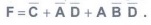 AU: May-06
Ans. :
Q.5 What are don't care conditions and
incompletely specified functions ?
Ans. :Sometimes, while
designing a digital circuit, certain conditions of input are of no use.
Consider an example of BCD input for a seven segment display. In this case,
inputs from 0 through 9 are valid inputs. Thus, rest of the inputs from 10
through 15 do not signify anything at the output side. The outputs for which
inputs are not specified are called don't care outputs. The Boolean function in
which don't care outputs exists is called incomplete Boolean function or
incompletely specified functions.
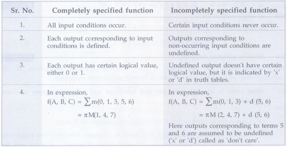
Q.6 Distinguish between completely
specified function and incompletely specified function.AU: May-09
Ans. :
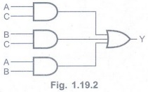
Q.7 Define a combinational logic
circuit. Give an example.
AU: May-08, June-16
Ans. : When logic
gates are connected together to produce a specified output for certain
specified combinations of input variables, with no storage involved, the
resulting circuit is called 'combinational logic circuit'.
A combinational circuit consists of
input variables, logic gates and output variables. For example, consider
following Boolean expression,
Y = AB + BC + AC
The combinational logic circuit for this
would require 3 AND gates and 1 OR gate as shown.
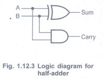
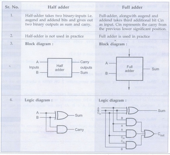
Q.8 Define half adder and full adder.
Ans. :
1) Half adder:
The logic circuit which performs the arithmetic sum of two bits is called a
half adder.
2) Full adder: The logic circuit which performs the arithmetic sum of 3 bits (bit 1 input 1, bit 2: input 2, bit 3: carry from the previous addition) is called a full adder.
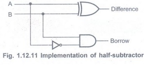
Q.9 Define half subtractor and full
subtractor.
Ans. :
1) Half subtractor:
It is a combinational circuit that subtracts two bits and produces their difference
and borrow.
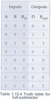
2) Full subtractor: It is a combinational circuit that performs a subtraction between 2 bits. It also takes into account borrow of the lower significant stage.
Q.10 Give the circuit of a half adder-subtractor. (Refer sections 1.12.1.1 and 1.12.2.1) AU: May-06
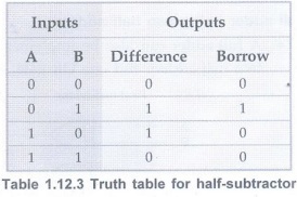
Q.11 Describe the truth table of a half
subtractor and write the Boolean expression corresponding to the difference and
the borrow. (Refer section 1.12.2.1)AU : May-05
A half-subtractor is a combinational circuit that subtracts two-bits and produces their difference.

• It also has an output to specify if a 1 has been borrowed.
• Let us designate minuend bit as A and the subtrahend bit as B. The result of operation A – B for all possible values of A and B is tabulated in Table 1.12.3.
• The Boolean expression for the outputs of half-subtractor can be determined as follows.
Q.12 Implement half adder using gates. (Refer section 1.12.1.1) AU: Dec.-07, May-10

Q.13 What is the difference between half
adder and full adder ?AU: Dec.-07
Ans.:
Q.14 What do you mean by carry
propagation delay ?
Ans. : Definition:
In parallel adders, sum and carry outputs of any stage cannot be produced until
the input carry occurs. This time delay in the addition process is called carry
propagation delay. This delay increases with increase in the number of bits to
be added in an adder circuit.
Q.15 Suggest a solution to overcome the
limitation on the speed of an adder.
AU: Dec.-09
Ans. :It is possible
to increase speed of adder by eliminating inter-stage carry delay. This method
utilizes logic gates to look at the lower-order bits of the augend and addend
to see if a higher-order carry is to be generated.
Q.16 How will you build a full-adder
using two half-adders and an OR gate ? (Refer section
1.12.1.2) AU: Dec.-02,14
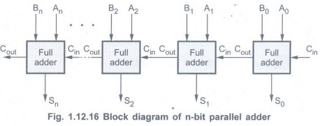
Q.17 Draw 4-bit binary parallel adder.
(Refer section 1.12.3) AU: Dec.-03
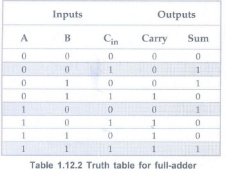
Q.18 Write down the truth table of a
full-adder. (Refer section 1.12.1.2) AU : May-04
Q.19 Write down the truth table of a
full-subtractor. (Refer section 1.12.2.2) AU : Dec-02,04,May-13
Q.20 Write down the truth table of half-subtractor.
(Refer section 1.12.2.1) AU: Dec.-03
Q.21 Draw the circuit of a half-adder.
(Refer section 1.12.1.1) AU: Dec.-05
Q.22 Write the truth table for a half-subtractor. (Refer section 1.12.2.1) AU: Dec.-05
Q.23 Construct a 4-bit binary to gray code converter circuit and operation. (Refer example 1.13.5) AU: May-06
Example: Design and implement a 8421 to gray code converter. Realize the converter using only NAND gates. AU: Dec.-05, 14, 16, May-06, 13, Marks 12
Solution :
Step 1: Form the Truth table relating 8421 binary code and Gray code
Input code: Binary code : B3 B2 B1 B0
Output code:Gray code: G3 G2 G1 G0
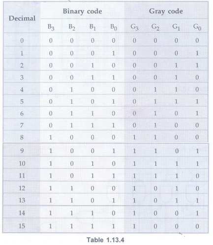
Step 2: K-map simplification for each gray code output
Step 3:Realization of code converter using XOR-gates

Step 4: Realization of code converter using NAND gates

For this converter we have derived the Boolean expressions for each gray code output in the sum of product (SOP) form. We can implement SOP expression using AND-OR logic or NAND-NAND logic. Let us see the implementation of code converter using NAND-NAND logic.
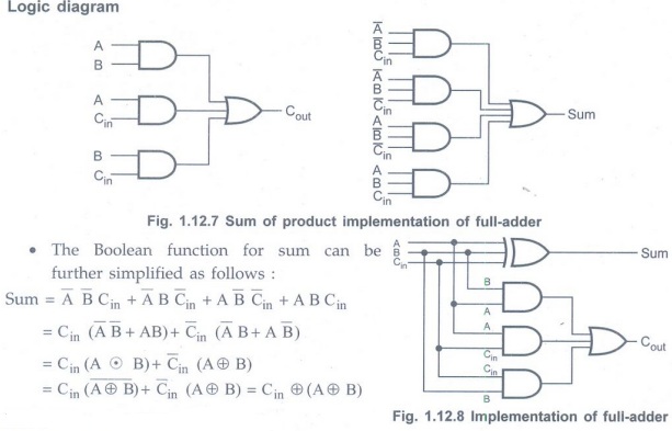
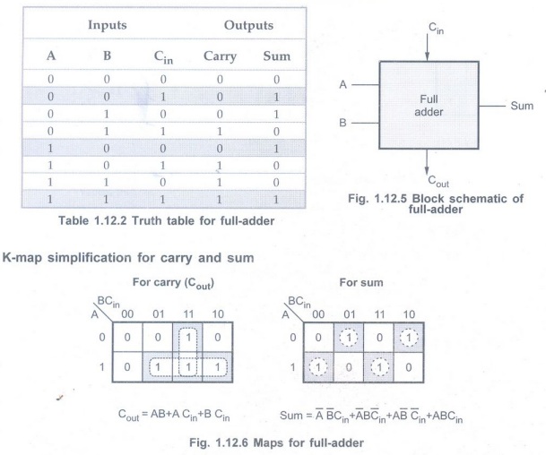
Q.24 What is a full-adder?
(Refer section 1.12.1.2) AU: May-07
• A full-adder is a combinational circuit that forms the arithmetic sum of three input bits.
• It consists of three inputs and two outputs.
• Two of the input variables, denoted by A and B, represent the two significant bits to be added. The third input Cin, represents the carry from the previous lower significant position.
• The truth table for full-adder is shown in Table 1.12.2.
Q.25 What is the need for code
conversion? Give two commonly used codes. (Refer section
1.13) AU: May-09
• There are different codes such as Binary-Coded-Decimal (BCD), Excess-3, Gray and so on. Many times it is required to convert one code to another.
• The procedure to design code converters :

Step 1:Write the truth table showing the relationship between input code and output code.
Step 2:For each output code bit determine the simplified Boolean expression using K-map.
Step 3:Realize the code converter using logic gates.
Q.27 What do you mean by magnitude
comparator? OR Write a short note on 1-bit comparator.AU:
Dec.-19
Ans. : It is a special
combinational circuit designed primarily to compare the relative magnitudes of two
binary numbers. An n-bit comparator receives two n-bit numbers, A and B,
outputs are: A > B, A = B and A < B. As per the magnitudes of the two
numbers, one of the outputs will be high.
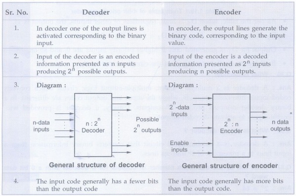
Q.28 What do you mean by encoder ?AU:
May-10
Ans. : An encoder is a
digital circuit that performs the inverse operation of a decoder. Encoder has
Q.29 Write a short note on priority encoder. OR What is a priority encoder ? AU: Dec.-14, 16, May-17
Ans.: A priority
encoder is an encoder circuit in which if two or more inputs are equal to 1 at
the same time, the input having the highest priority will take precedence.
• As per the table, when D3
is high, regardless of other inputs, the output is 11.
• D2 has next priority, thus,
with D2 =1 and D3= 0, output will be 10.
• Output for D1 is generated
only if higher priority inputs are 0, and so on.
•If all inputs are 0, two outputs of the
circuit are not used.
Q.30 What is decoder ?
Ans. : A decoder is a
multiple - input, multiple-output logic circuit which converts coded inputs
into coded outputs, where the input and output codes are different. In a binary
decoder n-inputs produce 2n outputs. Usually, a decoder is provided
with enable inputs to activate decoded output.
Q.31 What is binary decoder ?
Ans. : A decoder is a
combinational circuit that converts binary information from n input lines to a
maximum of 2n outputs lines.
Q.32 What will be the maximum number of
outputs for a decoder with a 6 bit data word ?AU: May-09
Ans. : 26 =
64
Q.33 Mention the uses of decoders.
(Refer section 1.15.4)AU: Dec.-06
The uses of decoders are :
• Code converters
• Implementaion of combinatonal circuits
• Address decoding
• BCD to 7-segment decoder
Q.34 Draw a 4 x 16 decoder constructed
with two 3 x 8 decoders. (Refer section 1.15)AU: May-07
• A decoder is a multiple-input, multiple-output logic circuit which converts coded inputs into coded outputs, where the input and output codes are different.
• The Fig. 1.15.1 shows the general structure of the decoder circuit.
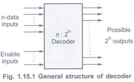
• The encoded information is presented as n inputs producing
• The 2n output values are from 0 through 2n - 1.
• Usually, a decoder is provided with enable inputs to activate decoded output based on data inputs. When any one enable input is unasserted, all outputs of decoder are disabled.
Q.35 What is a data selector? or what is
multiplexer ? or Why is MUX called as data detector ? AU: Dec.-06, May-11
Ans. :
• Multiplexer is a digital switch.
Particularly, it has 2n input lines and n selection lines whose bit
combinations determine which input line is selected and routed onto available
only single output line.
• Hence, multiplexer is a selector of
one out of several data sources available at its input lines, to connect it to
output line. Simply it is a 'many into one' device and also called 'data
selector'.
Q.36 Mention the differences between DMUX and MUX. (Refer section 1.18) AU: May-07, 09
Q.37 Give an application each for a
multiplexer and a demultiplexer. (Refer sections 1.17.7
and 1.18.4)AU: Dec.-08
Q.38 With a aid of block diagram clearly
distinguish between a decoder and encoder.
Ans. :
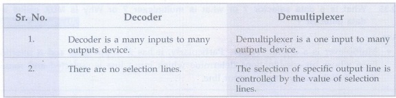
Q.39 Distinguish between a demultiplexer and decoder. AU: Dec.-03, 05, 09, May-04, 13
Ans. :
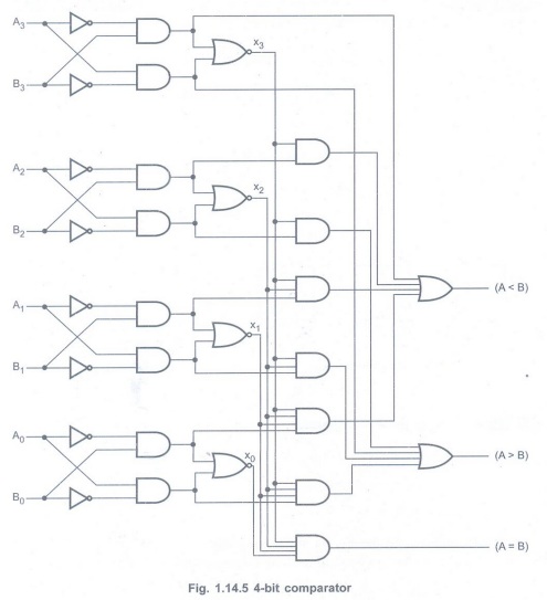
Q.40 Using a single IC 7485, draw the
logic diagram of a 4-bit comparator.
(Refer section 1.14.1)AU : May-03
IC 7485 is a 4-bit comparator. It can be used to compare two 4-bit binary words by grounding I (A < B), and I (A > B), and connector input I (A = B) to Vcc. These ICs, can be cascaded to compare words of almost any length. Its 4-bit inputs are weighted (A0 – A3) and (B0 – B3), where A3 and B3 are the most significant bits.
Q.41 What is a decoder and obtain the relation between the number of inputs 'n' and outputs 'm' of a decoder.
(Refer section 1.15)AU : May-05
• A decoder is a multiple-input, multiple-output logic circuit which converts coded inputs into coded outputs, where the input and output codes are different.
• The Fig. 1.15.1 shows the general structure of the decoder circuit.
• The encoded information is presented as n inputs producing
• The 2n output values are from 0 through 2n - 1.
• Usually, a decoder is provided with enable inputs to activate decoded output based on data inputs. When any one enable input is unasserted, all outputs of decoder are disabled.
Q.42 What are functions of encoders and decoders ?
(Refer Q.38)AU: Dec.-06
Q.43 What is a multiplexer ?
(Refer section 1.17)AU: Dec.-06, May-10
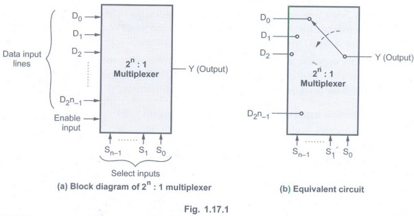
In digital systems, many times it is necessary to select single data line from several data-input lines, and the data from the selected data line should be available on the output. The digital circuit which does this task is a multiplexer.
It is a digital switch. It allows digital information from several sources to be routed onto a single output line, as shown in the Fig. 1.17.1. The basic multiplexer has several data-input lines and a single output line. The selection of a particular input line is controlled by a set of selection lines. Since multiplexer selects one of the input and routes it to output, it is also known as data selector. Normally, there are
Q.44 What is a priority encoder ? (Refer section 1.16.2) AU: May-07, 08, Dec.-10
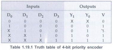
• A priority encoder is an encoder circuit that includes the priority function. In priority encoder, if two or more inputs are equal to 1 at the same time, the input having the highest priority will take precedence.
• Table 1.16.2 shows truth table of 4-bit priority encoder.

•Table 1.16.2 shows
•The
•The output for
•The output V (a valid output indicator) indicates, one or more of the inputs are equal to 1. If all inputs are 0, V is equal to 0, and the other two outputs
(
K-map simplification

Q.45 Mention any two applications of multiplexers. (Refer section 1.17.7) AU: May-07, 09
1. They are used as a data selector to select one out of many data inputs.
2. They can be used to implement combinational logic circuit.
3. They are used in time multiplexing systems.
4. They are used in frequency multiplexing systems.
5. They are used in A/D and D/A converter.
6. They are used in data acquisition systems.
Q.46 What is a demultiplexer ?
(Refer section 1.18)AU: May-08
Q.47 What is decoder ? Draw the block
diagram and truth table for 2 to 4 decoder. (Refer section
1.15)AU : May-09
• A decoder is a multiple-input, multiple-output logic circuit which converts coded inputs into coded outputs, where the input and output codes are different.
• The Fig. 1.15.1 shows the general structure of the decoder circuit.
• The encoded information is presented as n inputs producing
• The 2n output values are from 0 through 2n - 1.
• Usually, a decoder is provided with enable inputs to activate decoded output based on data inputs. When any one enable input is unasserted, all outputs of decoder are disabled.
Q.48 Determine the size and number of
multiplexers required to implement a full adder.AU : May-11
Ans. : We need two 8:
1 multiplexers to implement a full adder.
Q.49 Implement the following Boolean
function using 8:1 multiplexer
F(A, B, C)= Σm(1, 3, 5, 6) (Refer
section 1.17.7) AU: Dec.-14
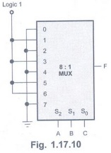
Implement the given function using 8 : 1 multiplexer.
F(A,B,C) = ∑m(1, 3, 5, 6). AU: Dec.-14, Marks 2
Solution :
Step 1: Select the multiplexer. Here, Boolean expression has 3 variables, thus we require 23 = 8:1 multiplexer.
Step 2: Connect inputs corresponds to the present minterms to logic 1.
Step 3: Connect remaining inputs to logic 0.
Step 4: Connect input variables to select lines of MUX.
Q.50 What is a priority Encoder?
(Refer Q.29) AU: Dec.-14
Q.51 Implement a full adder with 4 × 1 Multiplexer. (Refer example 1.17.14) AU: May-15
Implement full adder circuit using dual 4 to 1 multiplexer. AU: May-12, Dec.-14, Marks 8
Solution: Implementation tables :

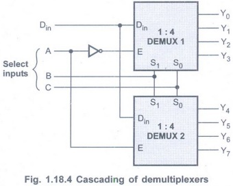
Design 1: 8 demultiplexer using two 1 : 4 demultiplexers.
Solution:
Step 1: Connect Din signal to in Din put of both the demultiplexers.
Step 2: Connect select lines B and C to select lines S1 and S0 of the both demultiplexers, respectively.
Step 3: Connect most significant select line (A) such that when A = 0 DEMUX 1 is enabled and when A = 1 DEMUX 2 is enabled.
Digital Principles and Computer Organization: Unit I: Combinational Logic : Tag: : Combinational Logic - Digital Principles and Computer Organization - Two marks Questions with Answers
Related Topics
Related Subjects
Digital Principles and Computer Organization
CS3351 3rd Semester CSE Dept | 2021 Regulation | 3rd Semester CSE Dept 2021 Regulation