Digital Principles and Computer Organization: Unit V: Memory and I/O
Parallel and Serial Interface
Memory and I/O - Digital Principles and Computer Organization
An I/O interface consists of circuits which connect an, I/O device to a computer bus.The interface can be classified as serial interface or parallel interface.
Parallel and Serial
Interface
• An I/O interface consists of circuits
which connect an, I/O device to a computer bus.
• As shown in Fig. 8.9.1 on one side of
the interface we have the bus signals for address, data and control. On the
other side we have a data path with its associated controls to transfer data
between the interface and the I/O device.

• The interface can be classified as
serial interface or parallel interface.
Parallel Interface
• Parallel interface is used to send or
receive data having group of bits (8-bits or 16-bits) simultaneously.
• According to usage, hardware and
control signal requirements parallel interfaces are classified as input
interface and output interface.
• Input interfaces are used to receive the
data whereas output interfaces are used to send the data.
Input Interface
• Commonly used input device is a
keyboard. Fig. 8.9.1 shows the hardware components needed for connecting a
keyboard to a processor.
• A typical keyboard consists of mechanical
switches that are normally open. When key is pressed, corresponding signal
alters and encoder circuit generates ASCII code for the corresponding key.
• For interfacing switches to the
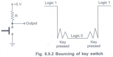
microprocessor based systems, usually push button keys are used. These push
button keys when pressed, bounces a few times, closing and opening the contacts
before providing a steady reading, as shown in the Fig. 8.9.2. Reading taken
during bouncing period may be faulty. Therefore, microprocessor must wait until
the key reach to a steady state; this is known as key debounce.
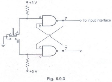
• Key-debouncing circuit included in the
block diagram of Fig. 8.9.3 eliminate effect of key bouncing. The problem of
key bounce can be eliminated using key debounce circuit (hardware approach) or
software approach.
• When debouncing is implemented in
software, the I/O routine that reads a ASCII code of character from the
keyboard waits long enough to ensure that bouncing has subsided.
• Fig. 8.9.3 shows the hardware approach
to prevent key bouncing. It consists of flip-flop. The output of flip-flop
shown in Fig. 8.9.3 is logic 1 when key is at position A (unpressed)and it is
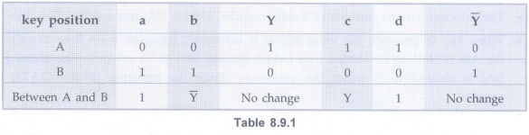
logic 0 when key is at position B, as shown in Table 8.9.1. It is important to
note that, when key is in between A and B, output does not change, preventing
bouncing of key output. In other words we can say that output does not change
during transition period, eliminating key debouncing.
• The output of encoder in Fig. 8.9.4
consists of the bits that represent the encoded character and one control
signal called valid, which indicates that a key is being pressed. The encoder
circuit sends this information to the interface circuit.
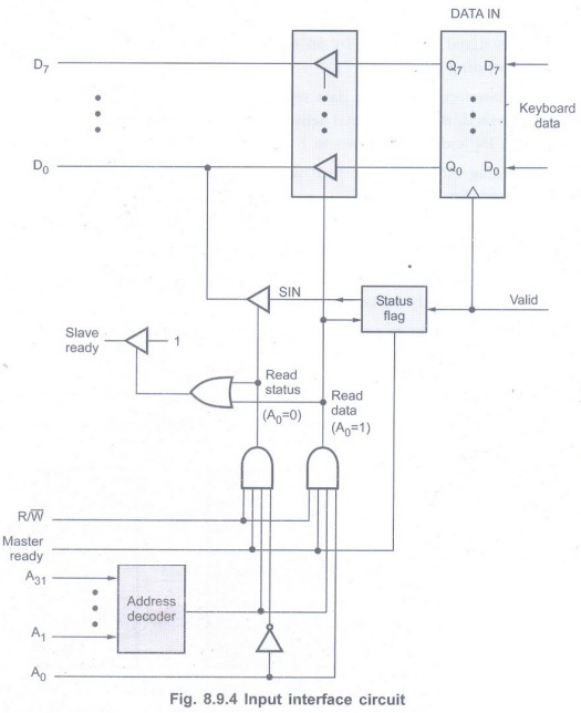
• The interface circuit consists of a
data register, DATA IN, and a status flag, SIN. •When key is pressed, the valid
signal is activated, (changes from 0 to 1) causing the ASCII code to be loaded
into DATA IN and SIN to be set to 1. The status flag SIN is cleared to 0 when
the processor reads the contents of the DATA IN register.
• The interface circuit is connected to
an asynchronous bus on which transfers are controlled by using the handshake
signals master-ready and slave-ready.
• The Fig. 8.9.4 shows the typical
internal circuitry for input interface. Here, we receive the data input from
the keyboard input device.
• When the key is pressed, its switch
closes and establishes a path for an electrical signal. This signal is detected
by an encoder circuit that generates ASCII code for the corresponding
character.
• The input interface consists of data
register, DATA IN, and status flag, SIN. When a key is pressed, the valid
signal activates and causes the ASCII code to be loaded into DATA IN and SIN to
be set to 1.
• The status flag SIN is cleared to 0
when the processor reads the contents of the DATA IN register.
• An address decoder is used to select the input interface when the high-order 31 bits of an address corresponds to any of the addresses assigned to this interface.
• Address bit
• The control handshake is accomplished
by activating the slave-ready signal when either Read-status or Read-data is
equal to 1.
Output Interface
• The Fig. 8.9.5 shows typical example of
output interface which is used to interface parallel printer.
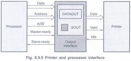
• The output interface contains a data
register, DATAOUT, and a status flag, SOUT.
• The SOUT flag is set to 1 when the
printer is ready to accept another character, and it is cleared to 0 when a new
character is loaded into DATAOUT by the processor.
• The Fig. 8.9.6 shows the detail
internal circuit for output interface.

Combined
Input/Output Interface
• Combine input and output interfaces is
shown in the Fig. 8.9.7.
• The 30-bits of higher order address (A31
- A2) are used to select overall interface. The low-order two
bits of address (A0 - A1) are used to select one of the
three addressable locations in the interface. These are: Two data registers and
one status register.
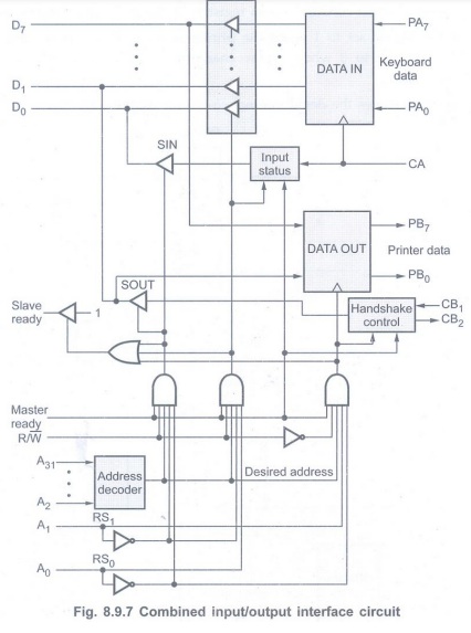
• Flags SIN and SOUT are in the status
register.
• Labels RS1 and S0 used
for inputs that determines the selection of desired register.
8.9.1.4 Programmable
Parallel Interface
• The input and output interfaces can be
combined into a single interface and the direction of data flow can be
controlled by data direction register.
• Single interface can be programmed to
use for input the data or output the data. Such a interface is known as
programmable parallel interface.
• The Fig. 8.9.8 shows the simplified
block diagram of 8-bit programmable parallel interface.

• Data and interface lines are
bidirectional. There direction is controlled by Data Direction Register (DDR).
• Two lines M0 and M1 are
connected to the status and control. These two lines decides the mode of
operation of the parallel interface, i.e. whether to operate parallel interface
as a simple input/output or handshake input/output.
• Ready and Accept signals are provided
as handshaking signals.
• The ![]() signal is also provided to
allow interrupt drives I/O data transfer.
signal is also provided to
allow interrupt drives I/O data transfer.
Serial Interface
• A serial interface is used to transmit / receive data serially, i.e,, one bit at a time.
• A key feature of an
interface circuit for a serial port is that it is capable of communicating in a
bit serial fashion on the device side and in a bit parallel fashion on the
processor side.
• A shift register is used to transform
information between the parallel and serial formats. The Fig. 8.9.9 shows the
block diagram of typical internal circuit for serial interface.
• As shown in the Fig. 8.9.9, the input
shift register accepts serial data bit by bit and converts it into the parallel
data. The converted parallel data is loaded in the data register and it is then
read by the processor using data bus.
• When it is necessary to send data
serially, the data is loaded into DATAOUT register. It is then loaded into
output shift register. Output shift register converts this parallel data into
serial data.

Comparison between Serial and Parallel Interface
• In parallel interface number of lines
required to transfer data depend on the number of bits to be transferred.
• For transmitting data over a long
distance, using parallel interface is impractical due to the increase in cost
of cabling.
• Parallel interface is also not
practical for devices such as cassette tapes or a CRT terminal. In such
situations, serial interface is used.
• In serial interface one bit is
transferred at a time over a single line.

Review Questions
1. What are the needs for input-output
interface?
2. Write a note on input interface.
3. Write notes on: Printer-processor
communication.
4. Explain the functions of a typical
8-bit parallel interface in detail.
5. How the parallel port output
interface circuit works?
6. Draw and explain the programmable
parallel interface.
7. Write a note on serial interface.
8. Compare between serial and parallel
interface.
Digital Principles and Computer Organization: Unit V: Memory and I/O : Tag: : Memory and I/O - Digital Principles and Computer Organization - Parallel and Serial Interface
Related Topics
Related Subjects
Digital Principles and Computer Organization
CS3351 3rd Semester CSE Dept | 2021 Regulation | 3rd Semester CSE Dept 2021 Regulation