Digital Principles and Computer Organization: Unit I: Combinational Logic
NAND-NAND Implementation
Combinational Logic - Digital Principles and Computer Organization
The implementation of a Boolean function with NAND-NAND logic requires that the function be simplified in the sum of product form.
NAND-NAND Implementation AU
May-05,09,10,12,15, Dec.-06,08,09
• The implementation of a Boolean
function with NAND-NAND logic requires that the function be simplified in the
sum of product form.
• The relationship between AND-OR logic
and NAND-NAND logic is explained using following example.
• Consider the Boolean function: Y =
ABC+DE+ F.
• This Boolean function can be
implemented using AND-OR logic, as shown in Fig. 1.8.1 (a).

• Fig. 1.8.1 (b) shows the AND gates are
replaced by NAND gates and the OR gate is replaced by a bubbled OR gate. The
implementation shown in Fig. 1.8.1 (b) is equivalent to implementation shown in
Fig. 1.8.1 (a), because two bubbled on the same line represent double inversion
(complementation) which is equivalent to having no bubble on the line.
• In case of single variable, F, the
complemented variable is again complemented by bubble to produce the normal
value of F.
• In Fig. 1.8.1 (c), the output NAND gate
is redrawn with the conventional symbol. The NAND gate with same inputs gives
complemented result, therefore ![]() is replaced by NAND gate with F
input to its both inputs. Thus all the three implementations of Boolean
function are equivalent.
is replaced by NAND gate with F
input to its both inputs. Thus all the three implementations of Boolean
function are equivalent.
Rules for obtaining the NAND-NAND logic
diagram
1. Simplify the given Boolean function
and express it in sum of product form (SOP form).
2. Draw a NAND gate for each product
term of the function that has two or more literals. The inputs to each NAND
gate are the literals of the term. This constitutes a group of first level
gates.
3. If Boolean function includes any
single literal or literals draw NAND gate for each single literal and connect
corresponding literal as an input to the NAND gate.
4. Draw a single NAND gate in the second
level, with inputs coming from outputs of first level gates.
Illustrative Examples

Example 1.8.2 Implement EX-OR gate using only NAND gates. AU: May-05, Dec.-06, 08, May-09, Dec.-09, Marks 2

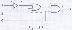
Example 1.8.3
Draw the logic diagram for the boolean expression ((A + B) C)'D using NAND
gates. AU Dec.-09, Marks 2
Solution:

Example 1.8.4
Implement the following Boolean function with NAND gates.
F(x, y, z) = (1, 2, 3, 4, 5, 7) AU May-10, 12, Marks 6
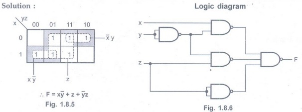
Example 1.8.5 Convert the following logic system into NAND gates only. AU May-15, Marks 8
Solution:
Procedure
1. Put bubbles at the inputs of OR gate
and bubble at the output of AND gate.
2. Compensate above change by putting
inverter for each bubble.
3. Remove double inversion.
4. Replace bubble - OR gate buy NAND
gate. Since 
5. Replace each NOT gate by NAND gate
with input shorted.

Digital Principles and Computer Organization: Unit I: Combinational Logic : Tag: : Combinational Logic - Digital Principles and Computer Organization - NAND-NAND Implementation
Related Topics
Related Subjects

Digital Principles and Computer Organization
CS3351 3rd Semester CSE Dept | 2021 Regulation | 3rd Semester CSE Dept 2021 Regulation