Digital Principles and Computer Organization: Unit V: Memory and I/O
Memory Technologies
Memory and I/O - Digital Principles and Computer Organization
Memories that consists of circuits capable of retaining their state as long as power is applied are known as static memories. These are Random Access Memory (RAM) and hence combinely called static RAM memories.
Memory Technologies
AU May-07, 08, 09, 12, 13, 15, Dec.-07,
08, 09, 10
RAM (Random Access Memories)
• Memories that consists of circuits
capable of retaining their state as long as power is applied are known as
static memories.
• These are Random Access Memory (RAM)
and hence combinely called static RAM memories.
Static RAM Cell
• The Fig. 8.3.1 shows the implementation
of static RAM cell. It consists of two cross-coupled inverters as a latch and
two transistors T1 and T2 which act as a switches.
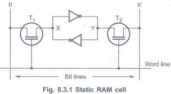
• The latch is connected to two bit lines
by transistors T1 and T2. The word line controls the
opening and closing of transistors T1 and T2. When word
line is at logic 0 level (Ground level), the transistors are off and the latch
retains its state.
Read operation
• For read operation, word line is made
logic 1 (high) so that both transistors are ON. Now if the cell is in state 1,
the signal on bit line b is high and the signal on bit line b' is low. The
opposite is true if the cell is in state 0. The b and b' are complements of
each other. The sense/write circuits connected to the bit lines monitor the
states of b and b' and set the output accordingly.
Write operation
• For write operation, the state to be
set is placed on the line b and its complement is placed on line b' and then
the word line is activated. This action forces the cell into the corresponding
state and write operation is completed.
CMOS Cell
• The Fig. 8.3.2 shows the CMOS cell.
Here, transistor pairs (T3, T5) and (T4, T6)
form the cross-coupled inverters and transistors T1and T2act
as a switches. The latch is connected to two bit lines by transistors T1 and
T2.
• The word line controls the opening and closing of transistors T1 and T2. When word line is at logic 0 level (ground level), the transistors T1 and T2 are off and the latch retains its state.
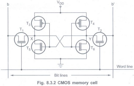
Read operation
• For read operation, word line is made
high to switch-on transistor T1 and T2. The cell is in
state 1, if voltage at point X is maintained high by having transistors T3 and
T6 on, while T3 and T5 are off. The cell is in
state 0, if the voltage at point X is maintained low by having transistors T3
and T6 off, while T4 and T5 are on.
Write operation
• For write operation, the state to be
set is placed on the line b and its complement is placed on line b', and then
the word line is activated. This action forces the cell into the corresponding
state.
DRAM (Dynamic RAMs)
• Dynamic RAM stores the data as a charge
on the capacitor. Fig. 8.3.3 shows the dynamic RAM cell.
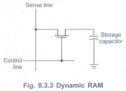
• A dynamic RAM contains thousands of
such memory cells.
• When COLUMN (Sense) and ROW (Control)
lines go high, the MOSFET conducts and charges the capacitor.
• When the COLUMN and ROW lines go
low,the MOSFET opens and the capacitor retains its charge. In this way, it
stores 1 bit.
• Since only a single MOSFET and
capacitor are needed, the dynamic RAM contains more memory cells as compared to
static RAM per unit area.
• The disadvantage of dynamic RAM is that
it needs refreshing of charge on the capacitor after every few milliseconds.
This complicates the system design, since it requires the extra hardware to
control refreshing of dynamic RAMs.
Comparison between SRAM and DRAM

(Read Only Memories)
• We can't write data in Read Only
Memories (ROM). It is non-volatile memory i.e. it can hold data even if power
is turned off.
• Generally, ROM is used to store the
binary codes for the sequence of instructions and data such as look up tables.
This is because this type of information does not change.
• ROMs are also accessed randomly with
unique addresses.
• The Fig. 8.3.4 shows the typical configuration
of a ROM cell. It consists of a transistor T and switch P.
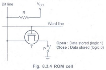
• The transistor T is driven by the word
line.
• The contents of cell can be read from
the cell when word line is logic 1.
• A logic value 0 is read if the
transistor is connected to ground through switch P. If switch P is open, a
logic value 1 is read.
• The bit line is connected through a
resistor to the power supply.
• A sense circuit at the end of the bit
line generates the proper output value. Data is stored into a ROM when it is
manufactured.
• There are four types of ROM Masked
ROM, PROM, EPROM and EEPROM or E2PROM.
PROM (Programmable
Read Only Memory)
• PROMS are programmed by user. To
provide the programming facility, each address select and data line intersection
has its own fused MOSFET or transistor.
• When the fuse is intact, the memory
cell is configured as a logic 1 and when fuse is blown (open circuit), the
memory cell is logical 0.
• Logical 0s are programmed by selecting
the appropriate select line and then driving the vertical data line with a
pulse of high current.
• Fig. 8.3.5 shows a PROM fused MOSFET
memory cell.
• The fuse uses material like nichrome and
polycrystalline. For blowing the fuse it is necessary to pass around 20 to 50
mA of current for period 5 to 20 μs. The blowing of fuses according to the
truth table is called programming of ROM.
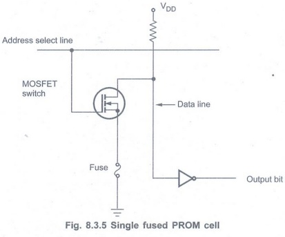
• The PROMS are onetime programmable.Once programmed,the information stored is permanent.
EPROM (Erasable Programmable Read Only Memory)
• Erasable programmable ROMs use MOS
circuitry. They store 1's and 0's as a
packet of charge in a buried layer of
the IC chip.
• EPROMs can be programmed by the user
with a special EPROM programmer.
• The important point is that we can
erase the stored data in the EPROMS by exposing the chip to ultraviolet light
through its quartz window for 15 to 20 minutes, as shown in the Fig. 8.3.6.

• It is not possible to erase
selective information, when erased the entire information is lost.
• The chip can be reprogrammed.
• This memory is ideally suitable for
product development, experimental projects and college laboratories, since this
chip can be reused many times.
EPROM Programming :
• When erased each cell in the EPROM
contains 1. Data is introduced by selectively programming 0's into the desired
bit locations. Although only O's will be programmed, both 1's and O's can be
presented in the data.
• During programming address and data are
applied to address and data pins of the EPROM. When the address and data are
stable, program pulse is applied to the program input of the EPROM. The program
pulse duration is around 50 ms and its amplitude depends on EPROM IC. It is
typically 5.5 V to 25 V.
• In EPROM, it is possible to program any
location at any time - either individually, sequentially or at random.
EEPROM
(Electrically Erasable Programmable Read Only Memory)
• Electrically erasable programmable ROMs
also use MOS circuitry very similar to that of EPROM.
• Data is stored as charge or no charge
on an insulated layer or an insulated floating gate in the device.
• The insulating layer is made very thin
(<200 Å). Therefore, a voltage as low as 20 to 25 V can be used to move
charges across the thin barrier in either direction for programming or erasing.
• EEPROM allows selective erasing at the
register level rather than erasing all the information since the information
can be changed by using electrical signals.
• The EEPROM memory also has a special
chip erase mode by which entire chip can be erased in 10 ms. This time is quite
small as compared to time required to erase EPROM. It can be erased and
reprogrammed with device right in the circuit.
Disadvantage
• EEPROMs are most expensive and the
least dense ROMs.
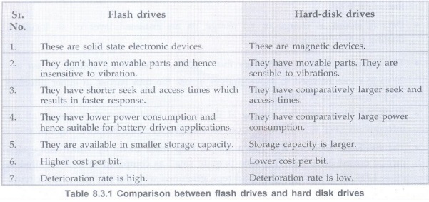
Flash Memory
Flash memories are read/write memories.
In flash memories it is possible to read the contents of a single cell, but it
is only possible to write an entire block of cells. A flash cell is based on a
single transistor controlled by trapped charge.
Flash devices have greater density than
the EEPROM memory. Due to this flash devices have higher capacity and a lower
cost per bit. They require a single power supply voltage and consume less power
in their operation. The low power consumption of flash memory makes it suitable
for portable equipments such as hand-held computers, cell phones, digital
cameras, MP3 music players and so on. In hand-hold computers and cell phones,
flash memory is used to store the software needed to operate the equipment. In
digital cameras, flash memory is used to store picture image data. In MP3
players, flash memory is used to store the sound data.
The flash memories are available in
modules. These modules are implemented in two types: flash cards and flash
drives.
Flash Cards:
In this, flash chips are mounted on a small card. Flash cards have a standard
interface that makes them usable in variety of applications. These cards are
available in variety of memory sizes. The sizes are 8, 32 and 64 Mbytes.
Flash Drives:
Flash drives are manufactured to replace hard-disk drives. These drives are
designed to fully emulate the hard disk, to the point that they can be fitted
into standard disk drive bays. However, the storage capacity of flash drives is
significantly lower than that of hard disk drives. Currently, the capacity of
flash drives is less than 1 Gbyte. The Table 8.3.1 shows the comparison between
flash drives and hard disk drives.
Synchronous DRAM (SDRAM)
• DRAMS whose operation is directly
synchronised with a clock signal are known as synchronous DRAMS or simply
SDRAMs.
• In a typical DRAM, the processor has to
wait through delay of access time slowing the system performance. To solve
above problem, the SDRAM exchanges data with the processor synchronized to an
external clock signal.
• Advantage:
This allows processor to read/write data with memory without imposing wait
states.
• In this, DRAM latches the address sent
by the processor and then responds after a set number of clock cycles.
• Advantage:
Meanwhile, the processor can do other task while the SDRAM is processing the
request.
• The Fig. 8.3.7 shows the internal
architecture of SDRAM. The cell organisation of SDRAM is same as asynchronous
DRAM. The address and data lines are buffered by means of buffer registers.
• It supports burst mode transfer.
• Advantage: In burst mode, after
first access, no address setup or row/column line pre-charge time is needed.
This improves system performance.
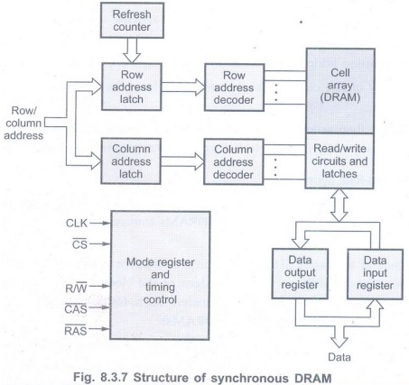
• Its mode register allows burst length,
burst type and latency to be customized to suit specific system needs.
• Advantage: The SDRAMs have
built in refresh circuitry.
• The Fig. 8.3.8 shows a timing diagram
for a typical burst read cycle of length 4.
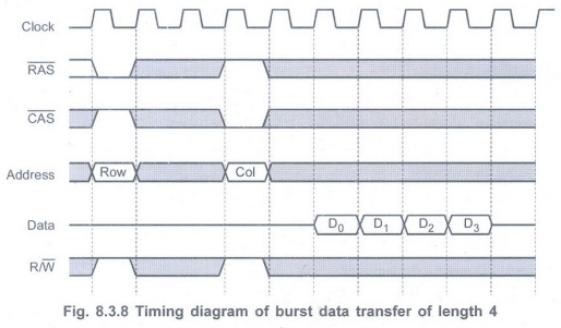
• The first clock cycle row address is
latched by activating RAS control signal. The memory typically takes 2 or 3
clock cycles to activate the selected row. (Fig. 8.3.8 shows 2 clock cycles).
• Then, the column address is latched by
activating the CAS control signal.
• After a delay of one clock cycle, the
memory places the first set of data bits on the data lines.
• The SDRAM then automatically
increments the column address to access the next three sets of data bits in the
selected row in three successive clock cycles.
Double-Data-Rate
Series
• The standard SDRAM performs its
operations on the rising edge of the clock signal. On the other hand, the
faster SDRAMs transfers data on both the edges of the clock signal.
• The latency of the faster SDRAMs is
same as that for standard SDRAM. However, since they transfer data on both the
edges of the clock signal, their bandwidth is effectively doubled for long
burst transfer. Such faster SDRAMs are known as Double-Data-Rate SDRAMs (DDR
SDRAMs).
• In DDR SDRAMs, the cell array is
organized in two banks as shown in Fig. 8.3.9.
• As shown in Fig. 8.3.9 it has dual bank
architecture to support on-chip parallelism.
• It also supports burst mode transfer.
This allows the sequential reading of number of bits from same row, eliminating
the address setup time for each bit.

• Each bank can be accessed separately.
• Consecutive words of a given block are
stored in different banks. Therefore, it is possible to transfer two words on
successive edges of the clock signal.
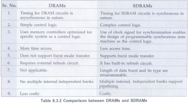
Comparison between
DRAMs and SDRAMs
Internal
Organization of Memory Chips
• Memory cells are organised in the form
of an array, in which each cell is capable of storing one bit of information.
Let us see the organisation of memory chip. using single decoder and using two
dimensional decoding.
Organization using
Single Decoder
• The Fig. 8.3.10 shows the organization
of 16 × 8 (16 words of 8-bit each) memory. Here, the organisation is shown with
detail connections of address lines, data lines and control lines. The data
input and the data output of each sense/write circuit are connected to a single
bidirectional data line that can be connected to the data bus of a computer.
Two control lines, , are provided in addition to address and data
lines. The
, are provided in addition to address and data
lines. The  input specifies the required operation and the
 ![]() input selects a given chip in a multichip memory system.
input selects a given chip in a multichip memory system.
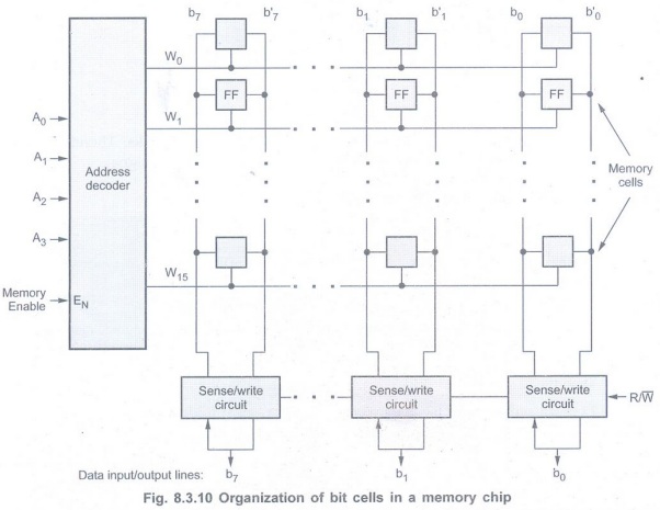
• As shown in the Fig. 8.3.10 there are
16 words of 8-bits each. A memory with 16 words needs four address lines. The
four address inputs go through a 4 × 16 decoder to select one of the sixteen
words. The decoder is enabled with a memory enable input. When the memory
enable is 0, all outputs of the decoder are 0 and none of the memory words are
selected. With the memory select at 1, one of the sixteen words is selected,
dictated by the value in the four address lines. Once a word has been selected,
the read/write input determines the operation. During write operation, the data
available in the input lines are transferred into the eight memory cells of the
selected word. The memory cells that are not selected are disabled and their
previous binary values remain unchanged.
Example 8.3.1
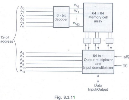
Draw the organization of 4 K×1 memory cell and explain.
Solution:
The Fig. 8.3.11 shows the organization of 4K×1 memory cell. Such organization needs12 address lines and
one data line, and two control signals (), resulting 15 external
connections. Here, 12-bit address is
divided into two groups of 6-bit each to
form therow and column addresses for the cell array. A row address selects a row of
64 cells, all of which are accessed in parallel. However, according to the
column address, only one of these cells is connected to the external data line
by the output multiplexer and input demultiplexer.
Review Questions
1. What are the types of RAMs? Explain
them in detail.
2. Describe the organization of a
typical RAM chip. AU May-07,Dec.-09, Marks 6
3. Write notes on static memories. AU:
Dec.-07, Marks 8
4. Describe the working principle of
RAM. AU: Dec.-08, Marks 6
5. Draw a CMOS memory cell and explain
its function. AU May-09, Marks 6
6. Write a note on asynchronous DRAM. AU:
Dec.-10, Marks 8
7. Differentiate DRAM and SRAM. AU:
Dec.-08, Marks 2
8. Write a note on synchronous DRAM. AU:
Dec.-10, Marks 8
9. Compare SDRAM with DDR SDRAM. AU
May-09, Marks 2
10. Explain synchronous DRAM technology
in detail. AU May-12, Marks 8
11. Draw the block diagrams of two types of DRAMs and explain. AU May-13, Marks 10
12. What is Rambus and Rambus channel?
13. Draw and explain the Rambus
interface using Rambus channel.
14. Explain the data transfer between
Rambus controller and slaves.
15. Write note on ROM technologies. AU:
Dec.-07, Marks 4
16. Give the features of a ROM cell. AU:
May-08, Marks 2
17. Briefly explain any four nonvolatile
memory in detail. AU: May-09, Marks 10
18. Write note on flash memory.
19. Compare flash drives with hard-disk
drives.
20. Elaborate on the various memory technologies and its relevance. AU: May-15, Marks 16
Digital Principles and Computer Organization: Unit V: Memory and I/O : Tag: : Memory and I/O - Digital Principles and Computer Organization - Memory Technologies
Related Topics
Related Subjects
Digital Principles and Computer Organization
CS3351 3rd Semester CSE Dept | 2021 Regulation | 3rd Semester CSE Dept 2021 Regulation