Digital Principles and Computer Organization: Unit II (a): Synchronous Sequential Logic
Latches
Synchronous Sequential Logic - Digital Principles and Computer Organization
SR latch which is 1-bit memory cell.Two inverters 3 and 4 are connected to enter the digital information.
Latches
AU: May-19
SR Latch
• Fig. 2.3.1 shows SR latch which is
1-bit memory cell.
• Two inverters 3 and 4 are connected to
enter the digital information.
• Input for gate 3 is S and input for
gate 4 is R. This latch is also called RS latch.
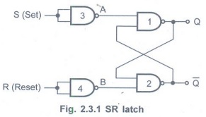
• For understanding the circuit
operation, we must first determine the output of NAND gate whose one of the
input is logic 0 and accordingly we have to determine the output of other NAND
gate in the cross coupled circuit.
• Because the output of NAND gate is 1
if any one input is 0.
• The circuit operation is as follows.
In Fig. 2.3.2, the output of shaded NAND gate is determined first, and the 0
input that decides the output of shaded NAND as 1 is shown in bold.
Case 1: S = R = 0
In this case, Ŝ = Ȓ = 1. If Q is 1, Q
and B inputs for NAND gate 2 are both 1 and hence output ![]() = 0.
Since
= 0.
Since ![]() = 0 and Ŝ = 1, the output of NAND gate 1 is 1,i.e. Q =
= 0 and Ŝ = 1, the output of NAND gate 1 is 1,i.e. Q =
If Q is 0, Q and Ȓ inputs for NAND gate
2 are 0 and 1 and hence output ![]() = 1. Since
= 1. Since ![]()
= 1 and Ŝ = 1, the output of NAND gate 1 is 0, i.e., Q = 0.
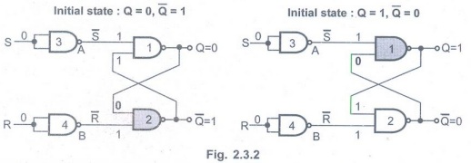
This shows that when S = R = 0, the
outputs do not change.
Case 2: S = 1 and R = 0
In this case, Ŝ = 0 and Ȓ =1. Since Ŝ = 0, the output of NAND
gate 1, Q = 1 (Recall that, for NAND any one or more input is 0, the output is
1) For NAND gate 2, both inputs Q and Ȓ
are 1, thus output ![]() = 0.
= 0.
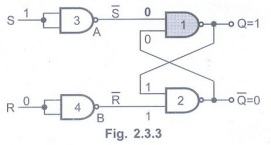
The inputs S = 1 and R = 0, makes Q = 1,
i.e., set state.
Case 3: S = 0 and R = 1
In this case, Ŝ = 1 and Ȓ = 0. Since Ȓ = 0, the output of NAND gate 2, ![]() = 1. For NAND gate 1,
both inputs
= 1. For NAND gate 1,
both inputs ![]() and Ŝ are 1, thus output Q = 0.
and Ŝ are 1, thus output Q = 0.
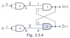
The inputs S = 0 and R = 1, makes Q = 0,
i.e., reset state.
Case 4: S = 1 and R = 1
When S = R = 1, both the outputs Q and ![]() try to become 1 which is not allowed and therefore, this input condition is
prohibited.
try to become 1 which is not allowed and therefore, this input condition is
prohibited.
Gated SR Latch
• In the SR latch output changes occur
immediately after theinput changes occuri.e. thelatch is sensitive to its S and
R inputs at all times.
• It can easily be modified to create a
latch that is sensitive to these inputs only when an enable input is active.
Such a latch with enable input is known as gated SR latch. It is as shown in
the Fig. 2.3.5.
• The Table 2.3.1 shows the truth table
for gated latch.

• As shown by truth table, the circuit
behaves like a SR latch when EN = 1 and retains its previous state when EN 0.
Gated D Latch
• For SR latch, when both inputs are same
the output either does not change or it is invalid (Inputs → 00, no change and
inputs → 11, invalid).
• In many practical applications, these
input conditions are not required.
• These input conditions can be avoided
by making them complement of each other.
• This modified SR latch is known as D
latch.
• Fig. 2.3.6 shows the D latch.
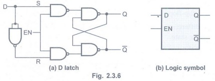
• The NAND gates 1, 2, 3 and 4 form the
basic SR latch with enable input.
• The fifth NAND gate is used to provide
the complemented inputs.
• As shown in the Fig. 2.3.6, D input
goes directly to the S input and its complement is applied to the R input,
through gate 5. Therefore, only two input conditions exists, either S = 0 and R
= 1 or S = 1 and R = 0.
• The truth table for D latch is as
shown in the Table 2.3.2.
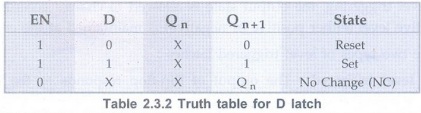
• As shown in the truth table, the Q
output follows the D input. For this reason D latch is sometimes called
transparent latch.
• Looking at the truth table for D latch
with enable input and simplifying Qn+1 function by k-map we get the
characteristic equation for D latch with enable input as 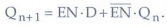 . This
is illustrated in Fig. 2.3.7.
. This
is illustrated in Fig. 2.3.7.
Review Questions
1. What is SR latch? Explain it's
operation.
2. What is gated SR latch?
3. Explain the working of gated D latch
with truth table and characteristic equation.
4. Draw the logic diagram and write the function table of D latch. AU May-19, Marks
Digital Principles and Computer Organization: Unit II (a): Synchronous Sequential Logic : Tag: : Synchronous Sequential Logic - Digital Principles and Computer Organization - Latches
Related Topics
Related Subjects
Digital Principles and Computer Organization
CS3351 3rd Semester CSE Dept | 2021 Regulation | 3rd Semester CSE Dept 2021 Regulation