Digital Principles and Computer Organization: Unit II (b): Analysis & Design of Clocked Sequential Circuits
Design of Clocked Sequential Circuits
Analysis & Design of Clocked Sequential Circuits - Digital Principles and Computer Organization
It is necessary to first obtain the state table from the given circuit information such as a state diagram, a timing-diagram, or other pertinent information.
Design of Clocked
Sequential Circuits
AU: Dec.-03,05,06,07,08,10,11,12,
May-07,08,09,10,11,15,17
• The recommended steps for the design
of a clocked synchronous sequential circuit are as follows :
1. It is necessary to first obtain the
state table from the given circuit information such as a state diagram, a
timing-diagram, or other pertinent information.
2. The number of states may be reduced
by state reduction technique if the sequential circuit can be categorized by
input-output relationships independent of the number of states.
3. Assign binary values to each state in
the state table, i.e. state assignment.
4. Determine the number of flip-flops
needed and assign a letter symbol to each.
5. Choose the type of flip-flop to be
used.
6.From the state table, derive the
circuit excitation and output tables.
7. Using the K-map or any other
simplification method, derive the circuit output functions and the flip-flop
input functions.
8.Draw the logic diagram.
State Reduction
• The state reduction technique
basically avoids the introduction of redundant states.
• The reduction in redundant states
reduce the number of required flip-flops and logic gates, reducing the cost of
the final circuit.
• The two states are said to be
redundant or equivalent, if every possible set of inputs generate exactly same
output and same nextstate.
• When two states are equivalent, one of
them can be removed without altering the input-output relationship.
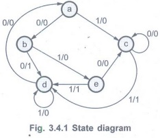
Example
•We start with a sequential circuit whose
specification is given in the state diagram of Fig. 3.4.1.
Step 1:Determine
the state table for given state diagram.
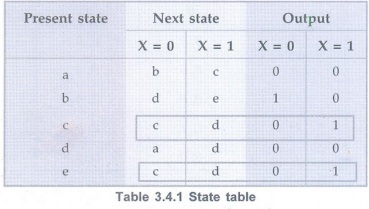
Table 3.4.1 shows the state table for
given state diagram.
Step 2:Find
equivalent states.
• Looking at the state table for two
present states that go to the same next state and have the same output for both
input combinations, we can easily find that states c and e are equivalent.
• This is because, c and e both states
go to states c and d and have outputs of 0 and 1 for X = 0 and X = 1,
respectively. Therefore, state e can be removed and replaced by c.
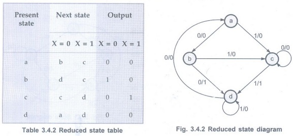
• The final reduced table is shown in
Table 3.4.2. The state diagram for the reduced table consists of only four
states and is shown in Fig. 3.4.2.
Examples for Understanding
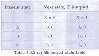
Example 3.4.1
Minimize the state table given below. AU Dec.-03, Marks 4
Solution :
Step 1:
Find equivalent states. The Table 3.4.3 shows the equivalent states in the
given state table. The states A and C, and states B and E generate exactly same
output and same next state. Hence, state A and C are equivalent and similarly
states B and E are equivalent.
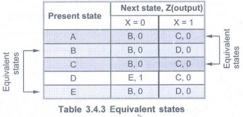
Step 2:
Replace redundant states with equivalent states.
Replace C by A and replace E by B, and
remove states C and E.
Now, there are no equivalent states and
hence Table 3.4.3 (a) shows the minimized state table.
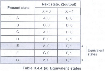
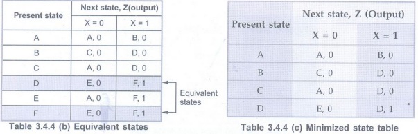
Example 3.4.2
Minimize the state table given below:AU: Dec.-05, Marks 6
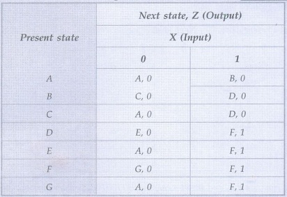
Solution:
Step 1:
Find equivalent states
Step 2:Replace
redundant state with equivalent state.
Therefore, replace G by E and remove
state G. Looking at Table 3.4.4 (b), we find that states D and F are
equivalent.
Therefore, replace F by D and remove
state F. Now, there are no equivalent states and hence Table 3.4.4 (c) shows
the minimized state table.
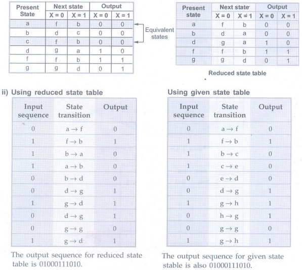
Example 3.4.3
i) Reduce the number of states in the following state table and tabulate the reduced
state table.
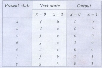
ii) Starting from state a, and input
sequence 01110010011, determine the output sequence for the given and reduced
state table.
AU Dec.-07, 11, May-10, Marks 16
Solution: i)
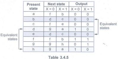
According to given state table we have states b and e, and states d and h are equivalent.
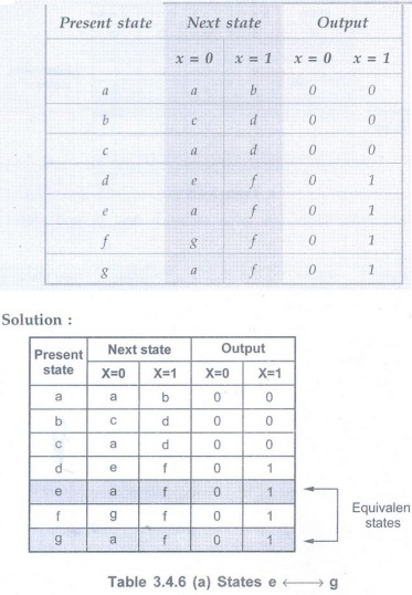
Example 3.4.4
Reduce the number of states in the following state diagram. Tabulate the
reduced state table and draw the reduced state diagram.
AU May-15, Marks 8
Reduction of State Table using Merger Graph
Merger graphs is state reducing tool
used to reduce states in the incompletely specified machine. The merger graph
is defined as follows :
1. It contains the same number of
vertices as the state table contains states. Refer Fig. 3.4.4.
2. Each compatible state pair is
indicated by a line drawn between the two state
vertices.
3. Every potentially compatible state
pair, with outputs not in conflict but whose next states are different, is
connected by a broken line. The implied states are drawn in the line break
between the two potentially compatible states.
4. If two states are incompatible, no
connecting line is drawn.
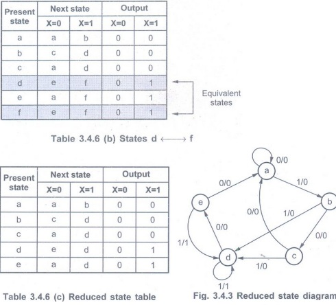
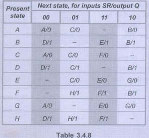
Example 3.4.5
Reduce the state table shown in Table 3.4.7 using Merger graph method.
Solution :
1. States A and B are compatible. Thus
the line isdrawn between A and B.
2. State A and C are compatible. Thus
the line is drawn between A and C.
3. State B and C are compatible. Thus,
the line is drawn between B and C.
4. States A and D are compatible only if implied states C and E are compatible. This is indicated by drawing a broken line between A and D with CE written in between.
5. States A and E are incompatible since
there outputs are different, so line is not drawn between A and E. For the same
reason states B, C and D are also not compatible with E.
6. State B and D are compatible. Thus,
the line is drawn between B and D.
7. States C and D are compatible only if
implied states C and E are compatible. This is indicated by drawing a broken
line between C and D with CE written in between.
8. It is found that states C and E are
not compatible and hence states A and D, and states D and C are also not
compatible. This is indicated by cross (X) marks.
The compatibility lines of merger graph
form a geometrical pattern consisting of one triangle (A, B, C), a line (B, D)
and a single state E that is not compatible with any others. Thus maximum
compatibles are:
(A, B, C) (B, D) (E)
Here, we can notice that state B is
common in two sets. However, it can be compatible with either states A and C or
state D, but not both. If we consider the next don't care state of B as state
C, it is compatible with stable A and C. If we consider the next don't care
state of B as state E it is compatible with state D.
Considering state B compatible with
states A and C, we have following set of maximum compatibilities for given
state table
(A, B, C) (D) (E)
Considering state B compatible with
state D, we have following set of maximum compatibilities for given state
table.
(A, C) (B, D) (E)
So we can say that there may be more
than one possible way of merging rows when reducing a state table.
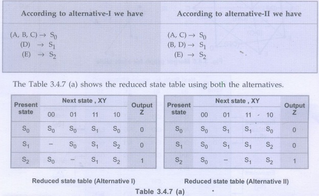
Example 3.4.6
(a) Reduce the given state table.
Solution :
Fig. 3.4.5 shows the merger graph. Each compatible state pair is indicated by a
line drawn between the two states vector.
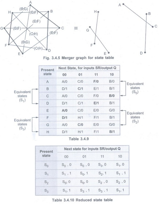
Every potentially compatible state pair, with outputs not in conflict but whose next states are different, is connected by a broken line. The implied states are drawn in the line break between the two potentially compatible states. If two states are incompatible, no connecting line is drawn.
Therefore, we have
(A, C) → S0
(B, D) → S1
(E, G) → S2
(F, H) → S3
The Table 3.4.10 shows the reduced
primitive flow.
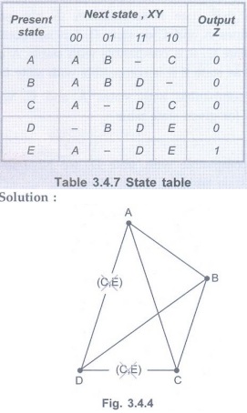
Reduction of State Table using Merger Table
When performing state reduction of
machines having a large number of states, it may be more convenient to find the
compatible pair and their implications in a merger table of the form
illustrated in Fig. 3.4.6, instead of using the merger graph. The merger table
method is also called as Paull-Unger method or implication chart method. The
table shows the state table for sequential machine and its merger table in the
Fig. 3.4.6.
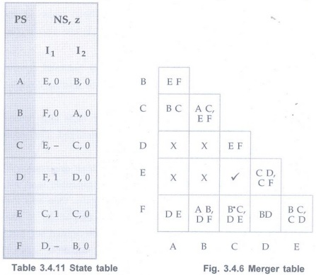
• Each cell of the merger table
corresponds to the compatible pair represented by the intersection of the row
and column headings.
• The incompatibility of two states is
indicated by placing cross mark X in the corresponding cell, while their
compatibility is indicated by placing check mark (✓)
in the cell.
• For example, states A and D are
incompatible because their outputs are conflicting and hence the cell
corresponding them contain cross mark X. On the other hand, states C and E are
compatible and hence the cell corresponding them contain check mark ✓.
• The implied pair or pairs corresponding
to state-pair are written with the cell, as shown in the Fig. 3.4.6. For
example, states A and C are compatible only when implied states B and C are
compatible, therefore implied pair B C is written in the cell corresponding to
states A and C.
• In the similar way the entire merger
table is written.
• Now it is necessary check whether
implied pairs are compatible or not. This can be checked by observing the
merger table. The implied states are incompatible if corresponding cell contain
X. For example, implied pair BD is incompatible because cell BD contain X. Since
BD is incompatible, states D and F are also incompatible. As DF is compatible,
states B and F are also incompatible. It is indicated by cross mark in Fig.
3.4.6.
• Once the merger table is completed, the
set of all maximal compatibles can be found by procedure which is counter part
to that of finding complete polygon in the merger graph. The procedure is as
follows:
1. Begin with right most column in the
merger table and proceed left unit a column containing a compatible pair is
encountered. For example, the pair EF in the merger table shown in Fig. 3.4.6.
2. Proceed left to the next column
containing at least one compatible pair. If the state to which this column
corresponds is compatible with all the states in the set of previously
determined compatible states then add this state to that set of compatible
states to form a larger compatible. If the state is not compatible with all the
states of previously determined set, but is compatible with some other state,
form a new set of compatible states. For example, state D is not compatible
with both E and F which are previously determined set of states. However, it is
compatible with state E. Therefore, it is not added in the previous set, but
the new set is formed, DE. On the other hand, state C is compatible with both E
and F which are previously determined set of states and hence it is included in
that set to form a new set CEF. Similarly, C is also included in set DE to get
a new set CDE.
3. Repeat step 2 until the left most
column is reached.
• After application of above mentioned
procedure the merger table in Fig. 3.4.6, gives following set of maximal
compatibles.
Column E: (E, F)
Column D: (E, F); (D, E)
Column C: (C, E, F); (C, D, E)
Column B: (C, E, F); (C, D, E); (B, C)
Column A: (C, E, F); (C, D, E); (A, B,
C); (A, C, F)
• The right most column is E. It
indicates that the state E is compatible with state F, resulting a compatible
pair (EF). The column D indicates that the state D is compatible with state E,
thus compatible pair (DE) is included in the compatible list. The column C
shows that the state C is compatible with states D, E and F and consequently
the compatibles generated previously are enlarged to include state C. The
column B consists of a single compatible pair (BC), which is added to the previously
generated compatible list. The column A indicates that the state A is
compatible with states B, C and F. Thus, the previously generated compatible
pair (BC) is enlarged to give the compatible (ABC), while rows C and F,
together with previously available compatibility relations, give the compatible
(ACF).
• Therefore, the set of maximal
compatibles is
(C, E, F); (C, D, E); (A, B, C); (A, C,
F)
State Assignment
• To determine the flip-flop input
functions, it is necessary to represent states in the state diagram using
binary values instead of alphabets.
• This procedure is known as state
assignment.
• We must assign binary values to the
states in such a way that it is possible to implement flip-flop input functions
using minimum logic gates.
Fig. 3.4.2 shows the state assignments
for the state diagram shown in Fig. 3.4.2.
Rules for state assignments
• There are two basic rules for making
state assignments.
Rule 1:
States having the same NEXT STATES for a given input condition should have
assignments which can be grouped into logically adjacent cells in a K-map.
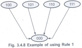
• Fig. 3.4.8 shows the example for Rule
1. As shown in the Fig. 3.4.8, there are fourstates whose next state is same.
Thus states assignments for these states are
000100, 101, 110 and 111 which can be
grouped into logically adjacent cells in a K-map.
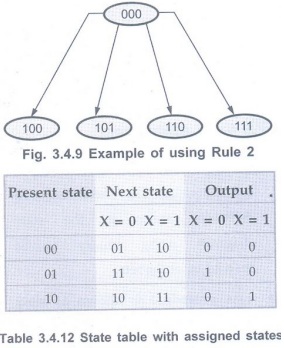
Rule 2:States
that are the NEXT STATES of a single state should have assignment which can be
grouped into logically adjacent cells in a K-map.
Fig. 3.4.9 shows the example for Rule 2.
As shown in the Fig. 3.4.9, for state 000, there are four next states. These
states are assigned as 100, 101, 110 and 111 so that they can be grouped into
logically adjacent cells in a K-map and table shows the state table with
assigned states.
Choice of Flip-Flops and Derivation of Next State and Output
• The most straightforward choice is to
use D flip-flops, because in this case the values of next state are simply
clocked into the flip-flops to become the new values of present state.
• For other types of flip-flops, such as
JK, T and RS the relationship between the next-state variable and inputs to a
flip-flop is not as straightforward as D flip-flop. For other types of
flip-flops we have to refer excitation table of flip-flop to find flip-flop
inputs. This is illustrated in the following example.
Example 3.4.7
A sequential circuit has one input and one output. The state diagram is shown
in Fig. 3.4.10. Design the sequential circuit with a) D flip-flops b) T
flip-flops c) RS flip-flops and d) JK flip-flops.
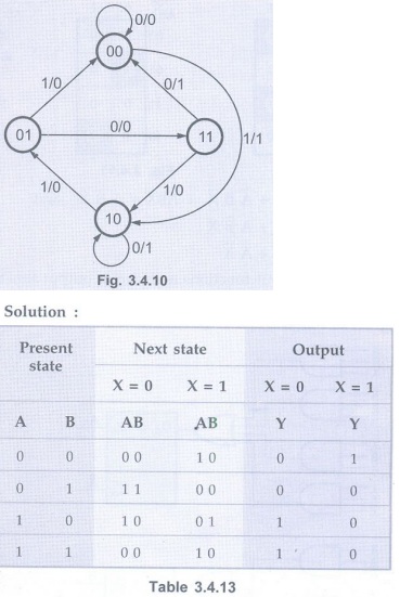
The state table for the state diagram shown in Fig. 3.4.10 is as given in Table
3.4.13.
As seen from the state table there are no
equivalent states. Therefore, no reduction is the state diagram. The state
table shows that circuit goes through four states, therefore we require 2
flip-flops (number of states = 2m where m = number of flip-flops).
Since two flip-flops are required first is denoted as A and second is denoted
as B.
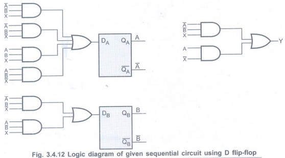
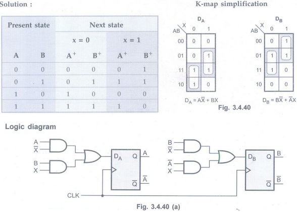
1. Design using D flip-flops
As mentioned earlier, for D flip-flops
next states are nothing but the new present states. Thus, we can directly use
next states to determine the flip-flop input with the help of K-map
simplification.
K-map simplification
For flip-flop A

With these flip-flop input functions and
circuit output function we can draw the logic diagram as follows
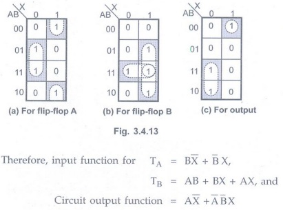
2. Design using T flip-flops
Using the excitation table for T
flip-flop shown in Table 3.4.14 we can determine the excitation table for the
given circuit as shown in Table 3.4.15.
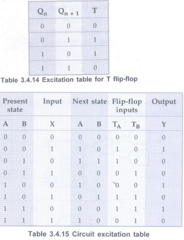
The first row of circuit excitation table shows that there is no change in the state for both flip-flops. The transition from 00 for T flip-flop requires input T to be at logic 0. The second row shows that flip-flop A has transition 0 → 1. It requires the input TA to be at logic 1. It requires the input TA to be at logic 1. Similarly, we can find inputs for each flip-flop for each row in the table byreferring present state, next state and excitation table.
Let us use K-map simplification to
determine the flip-flop input functions and circuit output functions.
K-map simplification
With these flip-flop input functions and
circuit output function we can draw the logic diagram as follows:
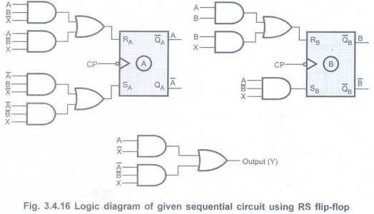
3. Design using RS flip-flops
Using the excitation table for RS
flip-flop shown in Table 3.4.16 we can determine the excitation table for the
given circuit as shown in Table 3.4.17.
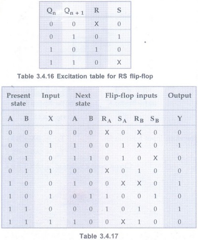
The first row of circuit excitation
table shows that there is no change in the state for both flip-flops. The
transition from 00 for RS flip-flop requires inputs R and S to be X and 0,
respectively. Similarly, we can determine inputs for each flip-flop for each
row in the table by referring present state, next state and excitation table.
Let us use K-map simplification to determine the flip-flop input functions and
circuit output functions.
K-map simplification
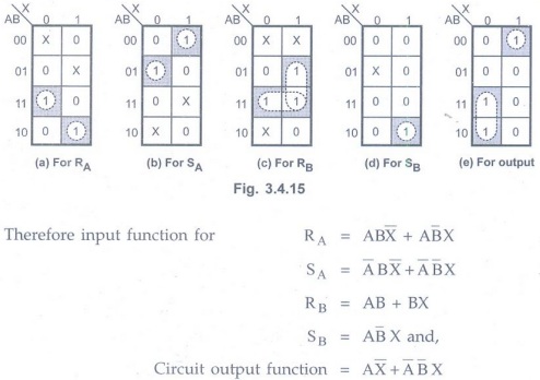
With these flip-flop input functions and
circuit output function we can draw the logic diagram as follows:
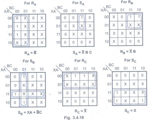
4. Design using JK flip-flops
Using the excitation table for JK
flip-flop shown in Table 3.4.18 we can determine the excitation table for the
given circuit as shown in Table 3.4.19.
The first row of circuit excitation
table shows that there is no change in the state for both flip-flops. The
transition from 00 for JK flip-flop requires inputs J and K to be 0 and X,
respectively. Similarly, we can determine inputs for each flip-flop for each
row in the table by referring present state, next state and excitation table.
Let us use K-map simplification to determine the flip-flop input functions and
circuit output functions.
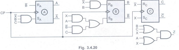
K-map simplification

Example 3.4.8
Design a sequential circuit using RS flip flops for the state table given below
using minimum number of flip flops. AU: Dec.-12, Marks 16
From example 3.4.2 we have minimized state table for given problem as shown in
the Table 3.4.19.
\Assigning a=000, b=001, c=010, d=011 and e=100 and referring excitation table for RS flip flop we have following excitation table.
K-map simplification
Logic diagram
Design with Unused States
• There are occasions when a sequential
circuit may use less than the available number of states. We can consider the
unused states as don't care conditions and can be used to simplify the input
functions to flip-flops.
• Let us consider one example. First we
will design the given sequential circuit without using unused states and then
we will design the given sequential circuit using unused states.
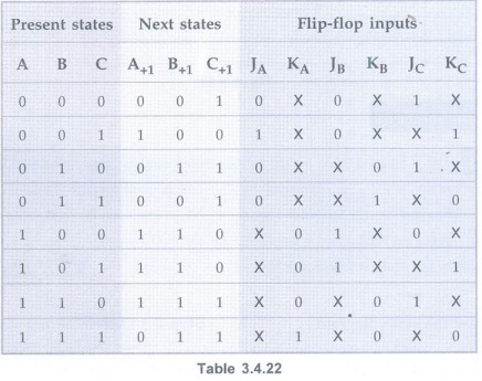
Example 3.4.9
Design the sequential circuit for the state diagram shown in Fig. 3.4.21 use JK
flip-flops.
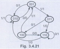
Solution :
Step 1:
Derive excitation table
The excitation table for given state
diagram is as follows
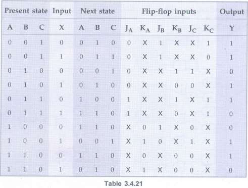
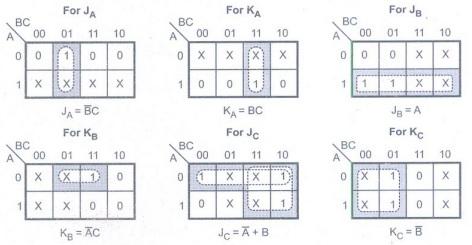
Step 2:
K-map simplification for JK inputs and circuit output
Step 3: Draw logic diagram.
Step 4:
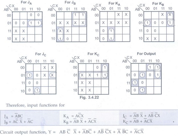
Derive circuit output and flip-flop inputs considering unused states.
Let us see the circuit design with the
use of unused states. These unused states 000, 101 and 111 are considered as a
don't cares and are used to simplify the K-maps as
follows:
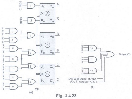
Step 5:Draw
logic diagram.
From the logic diagram it can be
realized that using unused state as don't cares we can further simplify the
flip-flop input functions and circuit output function.
Locked Condition
• In a counter if the next state of some
unused state is again an unused state and if by chance the counter happens to
find itself in the unused states and never arrived at aused state then the
counter is said to be in the lockoutconditions. This is illustratedin the Fig.
3.4.26.

• The counter which never goes in lockout
condition is called self starting counter. •The circuit that goes in lockout
condition is called brushless circuit.
• To make sure that the counter will come
to the initial state from any unused state, the additional logic circuit is
necessary.
• To ensure that the lock out does not
occur, the counter should be designed by forcing the next state to be the
initial state from the unused states as shown in Fig. 3.4.27.
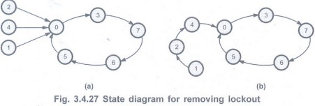
For example, as shown in Fig. 3.4.27,
actually it is not necessary to force all unused states into initial state.
Forcing any one state is sufficient. Because if counter initially goes to
unused state which is not forced, it will go to another unused state. This will
continue until it reaches the forced unused state. Once forced unused state is
reached next state is used state, and circuit is lock free circuit. This is
illustrated in Fig. 3.4.27 (b).
Example 3.4.10
Design a synchronous counter for
4→6→7→3 → 1 → 4...
Avoid lockout condition. Use JK type
design.
Solution :
Step 1:
State diagram
Here, states 5, 2 and 0 are forced to go
into 6, 3 and 1 state, respectively to avoid lockout condition.
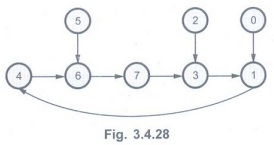
Step 2:
Excitation table
Step 3:
K-map simplification
Step 4:
Logic diagram
Examples with Solutions
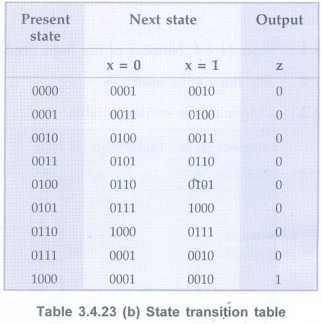
Example 3.4.11 For a four bit even parity bit generator, inputs come serially. The four bits of the input sequence are to be examined by the circuit and circuit produces a parity bit which is to be added in the original sequence. The circuit should get ready for receiving another four bits after producing a parity bit for the last sequence. Draw the state diagram and write down the state transition table. AU: May-08, Marks 10
Solution :
Step 1:
Draw the state diagram.
The state diagram for given problem is as
shown in the Fig. 3.4.30.
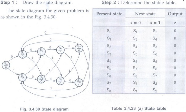
Step 3:Assign
states,
S0 = 0000,
S1 = 0001,
S2 = 0010,
S3 = 0011,
S4 = 0100,
S5 = 0101,
S6 = 0110,
S7 = 0111,
S8 = 1000.
Step 4: Determine
the state transition table.
Example 3.4.12
Design a sequential circuit with 4 FF ABCD. The next states of B, C, D are
equal to the present states of A, B, C respectively. The next state of A is
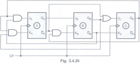
equal to the EX-OR of the present states of C and D. AU May-07, 09, Marks 16
Solution :
Example 3.4.13
Design a synchronous sequential circuit using JK for the given state
diagram. AU May-10, Marks 16
Solution:
Step 1:
Since N = 4. Number of flip-flops needed=2
Step 2:Flip-flops
to be used : JK
Step 3:Determine
the excitation table.

Step 4:
K-map simplification
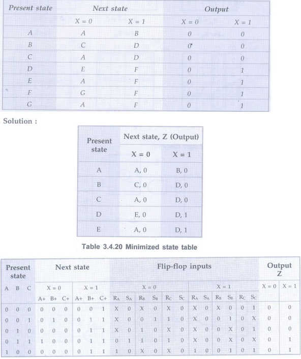
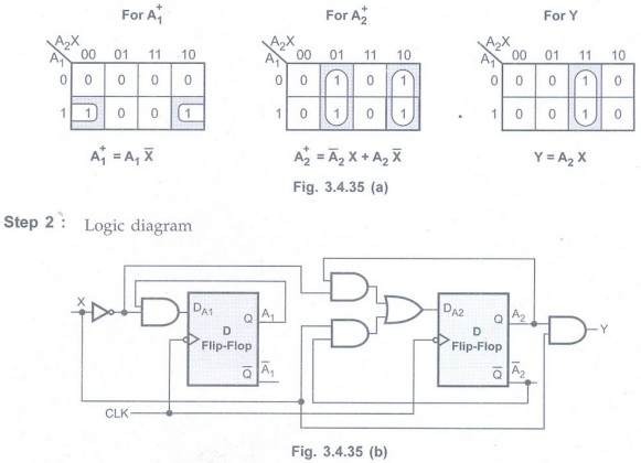
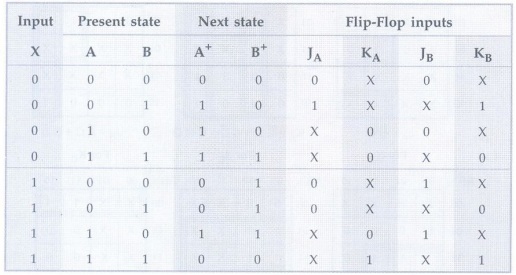
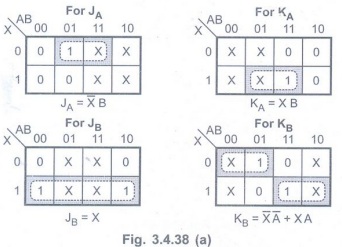
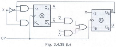
Example 3.4.14 Design the sequential circuit whose state table is given as AU: Dec.-07, Marks 16
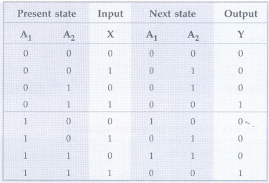
Solution:
Let us design sequential circuit using D flip-flop.
Step 1:
K-map simplification
Example 3.4.15
Design a sequential circuit with JK flip flop to satisfy the following state
equations
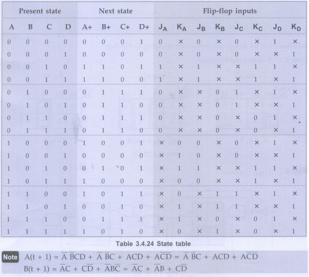
A(t + 1) = A'B'CD + A'B'C + ACD + AC'D'
B(t + 1) = A'C + CD' + A'BC'
C(t + 1) = B
D(t + 1) = D' AU: Dec.-08, Marks 10
Solution :
Step 1:
Derive the state table from given state equations
Step 1:
K-map simplification
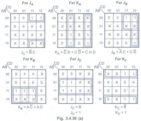
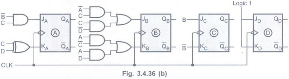
Step 3:Logic
diagram
Example 3.4.16
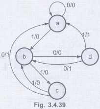
For the state diagram shown in Fig. 3.4.37, design a synchronous sequential
circuit using JK flip-flop. AU Dec.-10, Marks 16
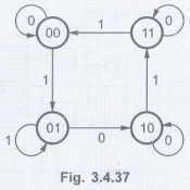
Solution :
Step 1:Excitation
table
Step 2:
K-map simplification
Step 3:Logic
diagram
Example 3.4.17
Design a clocked sequential machine using T flip-flops for the following state
diagram. Use state reduction if possible. Also use straight binary state
assignment. AU May-11, Marks 8
Solution :
Step 1:
Derive state table.
State table for the given state diagram
is a shown in Table 3.4.25 (a).
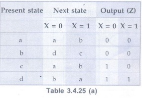
Step 2:
Derive excitation table.
Even though states a and same next states
for input X as the outputs are not same state reduction is not possible.
Using straight binary assignments as a =
00, b = 01, c = 10 and d table (Excitations table) is as shown in Table 3.4.25
(b).
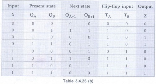
The flip-flop inputs and the circuit
outputs are
TA= f (QA, QB,
X)
TB= f (QA, QB,
X)
Z = f (QA, QB, X)
Step 3:K-map
simplification
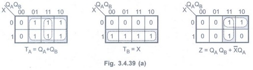
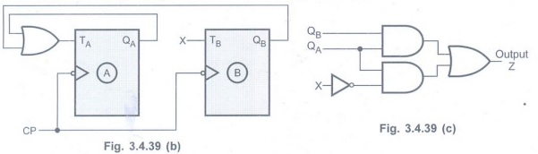
Step 4:
Logic diagram
Therefore, the logic diagram is as shown
in Fig. 5.4.39 (b).
Example 3.4.18
Design a sequential circuit with two D flip-flops A and B and an input x. When
x = O the state of the circuit remains the same. When x =1 the circuit goes
through the state transitions from 00 to 01 to 11 to 10 back to 00 and repeats. AU
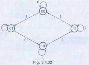
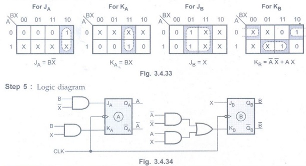
Dec.-11, Marks 10
Solution:
Examples for Practice
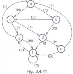
Example 3.4.19:Design
a clocked sequential circuit for state diagram shown in the Fig. 3.4.41.
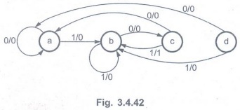
Example 3.4.20: Design a clocked sequential machine using JK flip-flops for the state diagram shown in Fig. 3.4.42. Use state reduction if possible. Make proper state assignment.
Example 3.4.21:
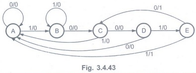
Design the sequential circuit using D flip-flops for the state diagram given in
Fig. 3.4.43.
Review Questions
1. Why is state reduction necessary? AU
Dec.-06, May-09, Marks 2
2. What is a self starting counter? AU
May-10, Marks 2
3. Explain the procedure of state minimisation
using Merger graph and Merger table.
4. Define state assignment. AU:
Dec.-05, Marks 2
5. Explain the steps involved in the reduction of state table. AU: Dec.-10, Marks 10
6. What are the significances of state
assignment? AU: May-17, Marks 2
Digital Principles and Computer Organization: Unit II (b): Analysis & Design of Clocked Sequential Circuits : Tag: : Analysis & Design of Clocked Sequential Circuits - Digital Principles and Computer Organization - Design of Clocked Sequential Circuits
Related Topics
Related Subjects

Digital Principles and Computer Organization
CS3351 3rd Semester CSE Dept | 2021 Regulation | 3rd Semester CSE Dept 2021 Regulation