Digital Principles and Computer Organization: Unit I: Combinational Logic
Decoders
Combinational Logic - Digital Principles and Computer Organization
A decoder is a multiple-input, multiple-output logic circuit which converts coded inputs into coded outputs, where the input and outputcodes are different.
Decoders AU
:Dec-06,08,11,12,18,May-07,09,11,15,19
• A decoder is a multiple-input, multiple-output
logic circuit which converts coded inputs into coded outputs, where the input
and output codes are different.
• The Fig. 1.15.1 shows the
general structure of the decoder circuit.
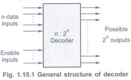
• The encoded information is presented
as n inputs producing
• The 2n output values are
from 0 through 2n - 1.
• Usually, a decoder is provided with
enable inputs to activate decoded output based on data inputs. When any one
enable input is unasserted, all outputs of decoder are disabled.
Binary Decoder
• A decoder which has an n-bit binary
input code and a one activated output out of 2n output code is
called binary decoder.
• A binary decoder is used when it is
necessary to activate exactly one of 2n outputs based on an n-bit
input value.
• Fig. 1.15.2 shows 2-to-4 decoder.
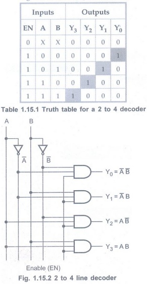
• 2 inputs are decoded into four
outputs, each output representing one of the minterms of the 2 input variables.
• The two inverters provide the
complement of the inputs, and each one of four AND gates generates one of the
minterms.
• The Table 1.15.1 shows the truth table
for a 2-to-4 decoder.
• If enable input is 1 (EN = 1), one,
and only one, of the outputs Y0 to Y3, is active for a
given input.
• The output Y0 is active,
i.e. Y0 = 1 when inputs A = B = 0, the output Y1 is
active when inputs A = 0 and B = 1.
• If enable input is 0, i.e. EN =0, then
all the outputs are 0.
Example 1.15.1
Draw the circuit for 3 to 8 decoder and explain.
Solution :Fig.
1.15.3 shows 3-to-8 line decoder. Here, 3 inputs are decoded into eight
outputs, each output represent one of the minterms of the 3 input variables.
The three inverters provide the complement of the inputs, and each one of the
eight AND gates generates one of the minterms. Enable input is provided to
activate decoded output based on data inputs A, B, and C. The table shows the
truth table for 3-to-8 decoder.

Expanding Cascading Decoders
• Binary decoder circuits can be
connected together to form a larger decoder circuit.
• Fig. 1.15.4 shows the 4 x 16 decoder
using two 3 x 8 decoders.
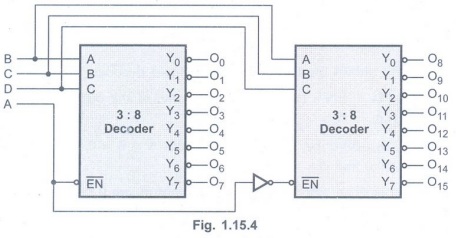
• Here, one input line (D) is used to
enable/disable the decoders.
• When D = 0, the top decoder is enabled
and the other is disabled. Thus the bottom decoder outputs are all 1s, and the
top eight outputs generate minterms 0 0 0 0 to 0 1 1 1.
• When D=1, the enable conditions are reversed and thus bottom decoder outputs generate minterms 1000 to 1111, while the outputs of the top decoder are all 1s.
Example 1.15.2 Design 5-to-32
decoder using one 2-to-4 and four 3-to-8 decoder ICs. AU Dec.-11, May-15,
Marks 16
Solution:
The Fig. 1.15.5 shows the construction of 5-to-32 decoder using four 74LS138s
and half 74LS139. The half section of 74LS139 IC is used as a 2-to-4 decoder to
decode the two higher order inputs, D and E. The four outputs of this decoder
are used to enable one of the four 3 to 8 decoders. The three lower order
inputs A, B and C are connected in parallel to four 3 to 8 decoders. This means
that the same output pin of each of the four 3-to-8 decoders is selected but
only one is enabled. The remaining enable signals of four 3-to-8 decoder ICs
are connected in parallel to construct enable signals for 5-to-32 decoder.
(See Fig. 1.15.5 on next page.)
Realization of Boolean Function using Decoder
• The combination of decoder and external
logic gates can be used to implement single or multiple output functions.
• When decoder output is active high, it
generates minterms (product terms) for input variables; i.e. it makes selected
output logic 1. In such case to implement SOP function we have to take sum of
selected product terms generated by decoder.

Examples for Understanding
Example 1.15.3
Implement Boolean function F = ∑ m (1, 2, 3, 7) using 3 : 8 decoder.
Solution :
Step 1:
Connect function variables as inputs to the decoder.
Step 2:
Logically OR the outputs correspond to present minterms to obtain the output.

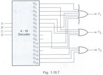
Example 1.15.4 Implement
the following multiple output combinational logic using a 4 line to 16 line
decoder.
Solution:
Step 1:Write
the function in their minterm forms
Y1 = ∑ m (0, 3, 2, 6, 10, 11)
Y2 =∑ m (1, 4, 5, 13) Y3 =∑m (7, 14, 15)
Step 2:
Logically OR the outputs of decoder corresponding to the minterms in the
functions.
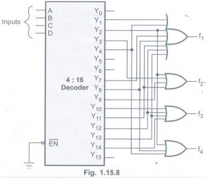
Example 1.15.5
Implement the following multiple output combinational logic circuit using a
4-line to 16-line decoder.
f1
= ∑m (1, 2, 4, 7, 8, 11, 12, 13), f2
= ∑m (2, 3, 9, 11)
f3
=∑m (10, 12, 13, 14), f4 =
∑m (2, 4, 8) AU: Dec.-08, Marks 10
Solution :
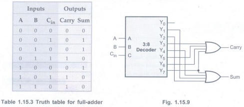
Example 1.15.6 Design and implement a full adder circuit using a 3: 8 decoder. AU May-11, Marks 5
Solution :
Truth table for full adder is as shown in the Table 1.15.3.
Examples for Practice
Example 1.15.7
Design an excess-3 to BCD code converter
using decoder and gates.
Example 1.15.8
Design 2×4 decoder using NAND gates.
Example 1.15.9
Design a combinational logic circuit
defined by the functions
F1 = a'b'c'd + a'c'd' + ab'cd', F2 =
a'b'c + b'cde' + a'bcde'
F3 = abcd' + ab'cd' + abcde'
Example 1.15.10
Implement the following multiple output function using suitable decoder.
f1 (A, B, C)= ∑ m(0, 4, 7)+d(2, 3)
f2 (A, B, C) = ∑ m(1, 5, 6)
f3 (A, B, C)= ∑ m(0, 2, 4, 6)
Applications of Decoders
The uses of decoders are :
• Code converters
• Implementaion of combinatonal circuits
• Address decoding
• BCD to 7-segment decoder
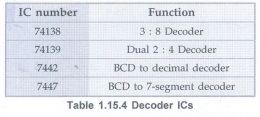
Decoder ICs
Review Questions
1. Define decoder.
2. Define binary decoder.
3. Explain the working of 2: 4 binary
decoder.
4. Draw a 4 x 16 decoder constructed with two 3 x 8 decoders. AU: May-07, Dec.-12, Marks 2
5. State the procedure to implement Boolean
function using decoder.
6. Mention the uses of decoders. AU
Dec.-06, Marks 2
7. What is decoder? Draw the block diagram and truth table for 2 to 4 decoder. AU May-09, 19, Marks 2
8. Explain in detail about decoders. AU:
Dec.-18, Marks 6
Digital Principles and Computer Organization: Unit I: Combinational Logic : Tag: : Combinational Logic - Digital Principles and Computer Organization - Decoders
Related Topics
Related Subjects
Digital Principles and Computer Organization
CS3351 3rd Semester CSE Dept | 2021 Regulation | 3rd Semester CSE Dept 2021 Regulation