Introduction to Operating Systems: Unit I: Introduction
Computer System
Introduction - Introduction to Operating Systems
Computer system consists of hardware device and software that are combined to provide a tool to user for solving problems.
Unit I: Introduction
Syllabus
Computer System - Elements and organization; Operating System Overview - Objectives and Functions - Evolution of Operating System; Operating System Structures - Operating System Services User Operating System Interface - System Calls - System Programs - Design and Implementation - Structuring methods.
Computer System
AU May-17, 18, 22, Dec-17
• Computer system consists of hardware device and software that are combined to provide a tool to user for solving problems.
• Fig. 1.1.1 shows modern computer system.

• Modern computer consists of one or two
CPU with main memory and various I/O devices. Common bus is used for
communication between these devices. Each device has its own device controller.
• CPU and device controller uses memory
cycle for execution purposes. But memory cycle is only available to one device
at a time.
• Bootstrap program is loaded when user
start the computer. It initialies all the device connected to the computer
system and then loads required device drivers.
• After this, operating system loads in
the computer system. In UNIX OS, an 'init' is the first process which execute
by OS.
• Interrupt is software and hardware. It
is used to send signal to CPU. Software interrupt is sometime called system
call.
•
When interrupt is trigger, the CPU stops executing the instruction and control
is transfer to the fixed location. Starting address is stored at fixed location
where the service routine executes.
•
Interrupts do not alter the control flow of the process executing
on the processor.
Storage
structure
• Processor access the data from main
memory before executing any instruction. Main memory is also called Random
Access Memory (RAM).
• DRAM is used in main memory. Fig.
1.1.2 shows hierarchy of storage device.
•
At the top of the hierarchy, we have storage on the CPU registers. For
accessing the CPU, it is fastest form of storage.
• Cache memory capacity is less than 1
MB.
• User program and data are stored in the main memory. Main memory is volatile, so it can not stored permanently.
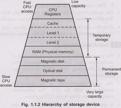
•
Storage system is classified as temporary storage or permanent
storage.
• Top level storage devices are low
capacity with faster CPU access and bottom level storage devices having very large capacity
with slow
CPU access speed.
I/O
structure
•
Every device uses a device controller to connect it to the computer's address
and data bus. Devices can be classified as a block oriented or character
oriented, depending on the number of bytes transferred on an individual
operation.
•
Storage devices are used to store data while the computer is off.
•
All the I/O devices are connected to each other by using common bus. CPU and
main memory is also connected with this bus.
•
Various types of controller is used in the computer system. Small Computer
System Interface (SCSI) controller can handle upto seven devices. Each device
controller have its own buffer.
• Device controller manage the data
transfer between peripheral device and its controller. Device driver is handled
by device controller.
I/O
operation steps
1. Device driver loads the registers
within the device controller.
2.
Device controller takes action according to the data loaded into the register.
3. Data is transfer from device to its
local buffer with the help of device controller.
4. After completion of data transfer,
the device controller sends an interrupt signal to device driver about data
transfer completion operation.
5. Then control goes to operating
system.
• The device driver is the operating
system entity that controls CPU-I/O parallelism. The software that communicates
with device controller is called device driver.
• A device can be started by the device
driver, and the application program can continue operation in parallel with the
device operation.
Instruction Execution
• The program which is to be executed is
a set of instructions which are stored in memory. The Central Processing
Unit (CPU) executes the instructions of the program to complete a task.
• The major responsibility of the
instruction execution is with the CPU. The instruction execution takes place in
the CPU registers.
• A special register contains the
address of the instruction. The CPU "fetches" the instruction from
memory at that address.
• The CPU "decodes" the instruction to figure out what to do. The CPU "fetches" any data b(operands) needed by the instruction, from memory or registers.
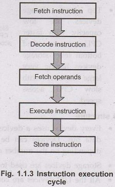
•
Fig 1.1.3 shows instruction execution cycle.
•
The CPU "executes" the operation specified by the instruction on this
data. The to CPU "stores" any results into a register or memory.
•The
register used for instruction execution are as follows:
1. Memory Address Register (MAR):
It specifies the address of memory location from which data or instruction is
to be accessed (for read operation) or to best yr which the data is to be stored
(for write operation).
2. Program Counter (PC):
It keeps track of the instruction which is to be executed next, after
the execution of an on-going instruction.
3.
Instruction Register (IR):
Here the instructions are loaded before their execution.
Interrupts
• Definition: It is an event external to the
currently executing process that causes a change in the normal flow of
instruction execution; usually generated by hardware not devices external to
the CPU. They tell the CPU to stop its current activities and not execute the
appropriate part of the operating system.
• Fig. 1.1.4 shows interrupts.
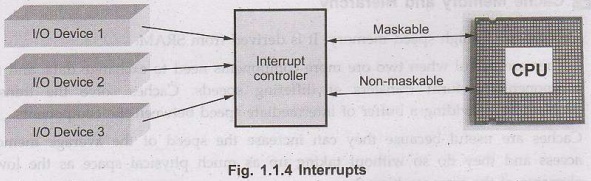
• The CPU uses a table and the interrupt
vector to find OS the code to execute in response to interrupts. When interrupt
signaled, processor executes a routine called an interrupt handler to deal with
the interrupt.
• Operating system may specify a set of instructions, called an interrupt handler, to be executed in response to each type of interrupt.
•
Interrupt Service Routine (ISR) is the software code that is executed when the
hardware requests interrupt. The design of the interrupt service routine
requires careful consideration of many factors. Although interrupt handlers can
create and use local variables, parameter passing between threads must be
implemented using shared global memory variables.
•
A private global variable can be used if an interrupt thread wishes to pass
information to itself, e.g., from one interrupt instance to another. The
execution of the main program is called the foreground thread, and the
executions of the various interrupt service routines are called background
threads.
• Interrupts
are of three types:
Hardware, software and trap.
•
Hardware Interrupts are generated
by hardware devices to signal that they need some attention from the OS. Software Interrupts are generated by programs when they want to request
a system call to be performed by the operating system.
•
Traps are generated by the CPU itself to indicate that some error or condition
occurred for which assistance from the operating system is needed.
•
Interrupt and trap numbers are defined by the hardware which is also
responsible for calling the procedure in the kernel space. An interrupt handler
is called in response to a signal from another device while a trap handler is
called in response to an instruction executed within the CPU.
•
Synchronous interrupts occur when a process attempts to perform an illegal
action, such as dividing by zero or referencing a protected memory location.
Synchronous interrupt occurs due to software execution.
Cache Memory and Hierarchy
•
Cache is small high speed memory. It is derived from SRAM.
• Caches are useful when two ore more components need to exchange data, and the components perform transfers at differing speeds. Caches solve the transfer problem by providing a buffer of intermediate speed between the components.
• Caches are useful because
they can increase the speed of the average memory access and they do so without
taking up as much physical space as the lower elements of the memory hierachy.
• Data is normally kept in storage
system.. when it required, it is copied into a faster storage system i.e. cache
memory for temporary basics.
• When user required a particular data, system check whether it is in the cache. If data found then, we use the data directly from the cache. It is not found then, use the data from the source.
• Internal programmable registers, such
as index registers, provide a high-speed cache for main memory. The programmer
implements the registor-allocation and register-replacement algorithms to
decide which information to keep in registers and which to keep in main memory.
• If the fast device finds the data it
needs in the cache, it need not wait for the 1er slower device. The data in the
cache must be kept consistent with the data in the components.
• If a component has data value change,
and the datum is also in the cache, the cache must also be updated. This is
especially a problem on multiprocessor systems where more than one process may
be accessing a datum.
• A component may be eliminated by an
equal sized cache, but only if the cache and the component have equivalent
state-saving capacity and the cache is affordable, because aster storage tends
to be more expensive.
• Unfortunately, cache also introduce an
additional level of complexity (coherency and consistency assurance).We also
incur an economic and space penalty when we add a cache.
•
Making a cache as large as a disk would be ineffective because it would be too
costly, the immense size would slow it down and a cache is generally a volatile
memory, while we want data on disks to be persistent..
• It holds data for temporary purpose to
reduce the time required to service I/O requests from the host. Fig. 1.1.5 shows
memory hierarchy.
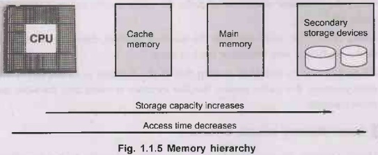
• Cache in CPU unit is referred as
Level1 cache (L1 cache) and cache stored in a chip next to CPU is termed as
Level2 cache (L2 cache) and it resides on the motherboard.
•
The function of cache is to act as a buffer between a relatively fast device
and a relatively slow one.
•
Small unit of allocation in cache is page. Cache is arranged into slots or
pages. It uses two components data store and tag RAM. The actual data is stored
in a
different
part of the cache, called the data store. The values stored in the tag RAM
determine whether a cache lookup results in a hit or a miss.
•
The size of the tag RAM determines what range of main memory can be
cached. Tag RAM is a small piece of SRAM
that stores the addresses of the data that is stored in the SRAM
•
A cache address can be specified simply by index and offset. The tag is kept
to allow the cache to translate from a
cache address to a unique CPU address.
• A cache hit means that the CPU tried
to access an address, and a matching cache
block was available in cache. So, the cache did not need to access RAM.
In a cache miss, the CPU tries to access an address, and there is no matching
cache block. So, the cache is forced to access RAM. of
• Cache includes tags to identify which
block of main memory is in each cache slot.
• Every cache block has associated with
it at least the modify and valid bits, and a tag address. The valid bit says if
the cache block is used or is unused. The modify bit makes sense only if
the valid bit is set. The modify bit says whether the data in the cache
block is different from RAM or is the same as RAM.
• The size of a page is dependent on the size of the cache and how the cache is organized. A cache page is broken into smaller pieces, each called a cache line. The size of a cache line is determined by both the processor and the cache design. .
• When the processor starts a read cycle, the cache checks to see
if that address is a cache hit.
• Cache Hit: If the cache contains
the memory location, then the cache will respond to the read cycle and
terminate the bus cycle.
•
Cache Miss: It is reference to item that is not resident in cache, but
is resident in main memory. For cache misses, the fast memory is cache and the slow memory is main memory.
Direct Memory Access Structure
•
Direct Memory Access (DMA) is one of several methods for coordinating the
timing of data transfers between an input/output (I/O) device and the core
processing unit or memory in a computer. DMA is one of the faster types of
synchronization mechanisms.
• Without DMA, the processor is
responsible for the physical movement of data between main memory and a device.
A special control unit may be provided to allow transfer of a block of data
directly between an external device and the main memory, without continuous
intervention by the processor. This approach is called direct memory access.
• Fig. 1.1.6 shows simplified diagram of DMA
controller.
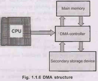
•
The DMA controller uses hold request (HOLD) and hold girl acknowledge (HOLD A)
signals to ask the CPU to stop driving the address, data and control buses so
that the DMA controller can drive them to carry out a transfer.
• A DMA controller implements direct memory access in a computer system. It connects directly to the I/O device at one end and to the system buses at the other end. It also interacts with the CPU, both via the system buses and two new direct connections.
•
Device controller transfers blocks of data from buffer storage directly to main
memory without CPU intervention. Only one interrupt is generated per block,
rather than the one interrupt per byte.
• The DMA controller may either stop the
CPU and access the memory or use the bus while the CPU is not using it
University
Questions
1. Discuss about direct memory
access.
2. Explain cache memory and its mapping. AU: May-17, Marks 6 AU: Dec.-17, Marks 13
3. Give reason why caches are
useful. What problems do they solve? What problems do they cause?
If a cache can be made as large as
the device for which it is caching why not make it that large and eliminated
the device? AU:
May-18, Marks 8
4.
Illustrate the flow of control with and without interrupts. AU: May-22, Marks 7
5.
Brief about the various types of memories in memory hierarchy. AU: May-22, Marks 6
Introduction to Operating Systems: Unit I: Introduction : Tag: : Introduction - Introduction to Operating Systems - Computer System
Related Topics
Related Subjects
Introduction to Operating Systems
CS3451 4th Semester CSE Dept | 2021 Regulation | 4th Semester CSE Dept 2021 Regulation