Digital Principles and Computer Organization: Unit I: Combinational Logic
Binary Adder Subtractor
Combinational Logic - Digital Principles and Computer Organization
The most basic operation, is the addition of two binary digits.The simple addition consists of four possible elementary operations
Binary Adder Subtractor
AU: Dec.-07.08,09,10,11,12,15,16,19,
May-03,06,09,10,11,12,13,15, 16,19
Adders
• The most basic operation, is the
addition of two binary digits.
• The simple addition consists of four
possible elementary operations, namely,
0+0=0
0+1 = 1
1 +0 = 1
1+ 1 = 102
• The first three operations produce a
sum whose length is one digit, but when the last operation is performed sum is
two digits. The higher significant bit of this result is called a carry, and
lower significant bit is called sum.
• The logic circuit which performs this
operation is called a half-adder.
• The circuit which performs addition of
three bits (two significant bits and a previous carry) is a full-adder.
Half Adder
• The half-adder operation needs two
binary inputs: augend and addend bits; and two binary outputs: sum and carry.
• The truth table shown in Table 1.12.1
gives the relation between input and output variables for half-adder operation.

Limitations of Half-Adder :
In multidigit addition we have to add
two bits along with the carry of previous digit addition. Effectively such addition
requires addition of three bits. This is not possible with half-adder. Hence
half-adders are not used in practice.
Example 1.12.1
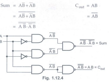
Draw half adder using NAND gates.
Solution:
For half adder:
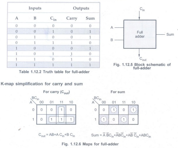
Full Adder
• A full-adder is a combinational circuit
that forms the arithmetic sum of three input bits.
• It consists of three inputs and two
outputs.
• Two of the input variables, denoted by A and B, represent the two significant bits to be added. The third input Cin, represents the carry from the previous lower significant position.
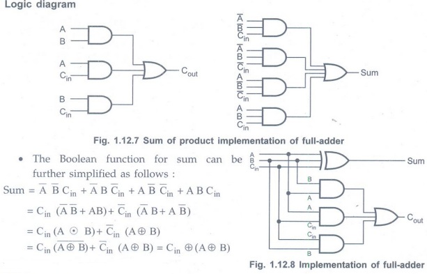
• The truth table for full-adder is
shown in Table 1.12.2.

Review Questions
1. Design half-adder using only NAND
gates.
2. Draw the truth table of half adder. AU
Dec.-15. Marks 2
3. Design full-adder using only NOR
gates.
4. Design full adder using two half
adders and OR gate. AU May-19, Marks 2
5. Design a full adder with inputs x, y, z and two outputs S and C. The circuits performs x + y + z, z is the input carry, C is the output carry and S is the sum. AU May-16, Marks 16
Subtractors
• The subtraction consists of four
possible elementary operations, namely,
0 0 = 0
0-1 = 1 with 1 borrow
1-0= 1
1-1 = 0
• In all operations, each subtrahend bit
is subtracted from the minuend bit.
• In case of second operation the minuend
bit is smaller than the subtrahend bit, hence 1 is borrowed.
Half Subtractor
• A half-subtractor is
a combinational circuit that subtracts two-bits and produces their difference.

• It also has an output to specify if a 1
has been borrowed.
• Let us designate minuend bit as A
and the subtrahend bit as B. The result of operation A – B for all possible
values of A and B is tabulated in Table 1.12.3.
• The Boolean expression for the outputs
of half-subtractor can be determined as follows.
Limitations of half-subtractor :
In multidigit subtraction, we have to
subtract two bits along with the borrow of the previous digit subtraction.
Effectively such subtraction requires subtraction of three bits. This is not
possible with half-subtractor.
Full Subtractor
• A full-subtractor is a combinational
circuit that performs a subtraction between two bits, taking into account borrow
of the lower significant stage.
• This circuit has three inputs and two
outputs.
• The three inputs are A, B and, Bin denote the minuend, subtrahend, and previous borrow, respectively.
• The two outputs, D and Bout represent the difference and output borrow, respectively.
• The Table 1.12.4 shows the truth table for full-subtractor.
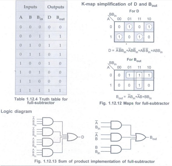
• The Boolean function for D (difference) can be further simplified as follows:
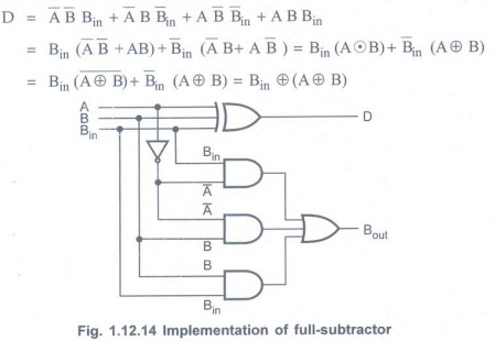
• full subtractor can also be
implemented with two half-subtractors and one OR gate, as shown in the Fig. 1.12.15.
• The difference output from the second
half-subtractor is the exclusive-OR of
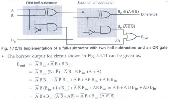
This Boolean function is same as borrow
out of the full-subtractor. Therefore, we can implement full-subtractor using
two half-subtractors and OR gate.
Review Questions
1. Explain the circuit diagram of
full-subtractor.
2. Design half subtractor and full
subtractor circuit and implement using NAND gate.
3. Design a full subtractor and derive
expression for difference and borrow. Realize using gates. AU: Dec.-15, Marks
16
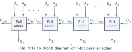
Parallel Adder
• In order to add binary numbers with
more than one bit, additional full-adders must be employed.
• A n-bit, parallel adder can be
constructed using number of full adder circuits connected in parallel.
• Fig. 1.12.16 shows the block diagram of
n-bit parallel adder using number of full-adder circuits connected in cascade,
i.e. the carry output of each adder is connected to the carry input of the next
higher-order adder.
• It should be noted that either a
half-adder can be used for the least significant position or the carry input of
a full-adder is made 0 because there is no carry into the least significant bit
position.
Example 1.12.2
Design a 4-bit parallel adder using full-adders.
Solution:
Fig.1.12.17 shows the block diagram for 4-bit adder. Here, for least significant
position, carry input of full-adder is made 0.

Review Question
1. Draw and explain the block diagram of
4-bit parallel adder.
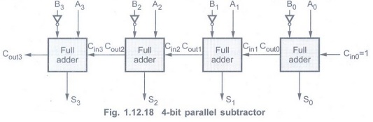
Parallel Subtractor
• The subtraction of binary numbers can
be done most conveniently by means of complements.
• The subtraction A-B can be done by
taking the 2's complement of B and adding it to A.
• The 2's complement can be obtained by
taking the 1's complement and adding one to the least significant pair of bits.
• The 1's complement can be implemented
with inverters and a one can be added to the sum through the input carry, as
shown in the Fig. 1.12.18.
Review Question
1. Draw and explain the block diagram of
4-bit parallel subtractor.
Parallel Adder / Subtractor
• The addition and subtraction operations
can be combined into one circuit with one common binary adder. This is done by
including an exclusive-OR gate with each full adder, as shown in Fig. 1.12.19.

• The mode input M controls the operation
of the circuit. When M = 0, the circuit is an adder, and when M = 1, the
circuit becomes a subtractor.
• Each exclusive - OR gate receives input
M and one of the inputs of B.
• The B inputs are all complemented and a
1 is added through the input carry.
• The circuit performs the operation A
plus the 2's complement of B, i.e. A - B.
• The parallel adder is ripple carry
adder in which the carry output of each full-adder stage is connected to the
carry input of the next higher-order stage. Therefore, the sum and carry outputs
of any stage cannot be produced until the input carry occurs; this leads to a
time delay in the addition process. This delay is known as carry propagation
delay.
• One method of speeding up this process
by eliminating inter stage carry delay is called look ahead-carry addition.
This method utilizes logic gates to look at the lower-order bits of the augend
and addend to see if a higher-order carry is to be generated.
Review Question
1. Design of 4 bit binary
adder-subtractor circuit. AU May-19, Dec.-19, Marks 8
Look-Ahead Carry Adder
The parallel adder discussed in the last
paragraph is ripple carry type in which the carry output of each full-adder
stage is connected to the carry input of the next higher-order stage.
Therefore, the sum and carry outputs of any stage cannot be produced until the
input carry occurs; this leads to a time delay in the addition process. This
delay is known as carry propagation delay, which can be best explained by
considering the following addition.
0101
0011 +
1000
Addition of the LSB position produces a
carry into the second position. This carry, when added to the bits of the
second position (stage), produces a carry into the third position. The latter
carry, when added to the bits of the third position, produces a carry into the
last position. The key thing to notice in this example is that the sum bit
generated in the last position (MSB) depends on the carry that was generated by
the addition in the previous positions. This means that, adder will not produce
correct result until LSB carry has propagated through the intermediate
full-adders. This represents a time delay that depends on the propagation delay
produced in an each full-adder. For example, if each full-adder is considered
to have a propagation delay of 30 ns, then S3 will not reach its
correct value until 90 ns after LSB carry is generated. Therefore, total time
required to perform addition is 90+30 = 120 ns.
Obviously, this situation becomes much
worse if we extend the adder circuit to add a greater number of bits. If the
adder were handling 16-bit numbers, the carry propagation delay could be 480
ns.
One method of speeding up this process
by eliminating inter stage carry delay is called look ahead-carry addition.
This method utilizes logic gates to look at the lower-order bits of the augend
and addend to see if a higher-order carry is to be generated. It uses two
functions: carry A- generate and carry propagate.
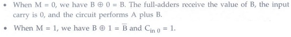
Consider the circuit of the
full-adders shown in Fig. 1.12.20. Here, we define two functions:carry generate
and carry propagate.
Gi is called a carry generate
and it produces on carry when both Ai and Bi are one,
regardless of the input carry. Pi is called a carry propagate
because it is term associated with the propagation of the carry from Ci
to
Ci+1
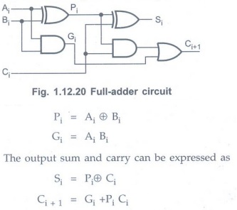
Now the Boolean function for the carry
output of each stage can be written as follows.
From the above Boolean function it can
beseen that C4 does not have to wait for C3 and C2
to propagate; in fact C4 is propagated at the same time as C2
and C3.
The Boolean functions for each output
carry are expressed in sum-of product form, thus they can be implemented using AND-OR
logic or NAND-NAND logic. Fig 1.12.21 shows implementation of Boolean functions
for C2, C3 and C4 using AND-OR logic.

Using a look ahead carry generator we
can easily construct a 4-bit parallel adder with a look ahead carry scheme.
Fig. 1.12.22 shows a 4-bit parallel adder with a look ahead carry scheme. As
shown in the Fig. 1.12.22, each sum output requires two exclusive-OR gates. The
output of first exclusive-OR gate generates Pi, and the AND gate
generates Gi.The carries are
generated using look ahead carry generator and applied as inputs to the second
exclusive-OR gate. Other inputs to exclusive-OR gate is pi. Thus
second exclusive-OR gate generates sum outputs. Each output each generated
after a delay of two levels of gate. Thus outputs S2 through S4
have equal propagation delay times.

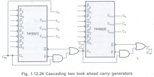
Example 1.12.3
Construct the look ahead carry generator to accommodate higher word size. AU:
Dec.-11, Marks 8
Solution:
Look ahead carry generators can be cascaded to increase the word size in
multiples of 4-bits. Fig. 1.12.24 shows the cascading two look ahead carry
generators (IC 74182s) to get word size of 8-bits.
Review Question
1. With neat diagram explain the 4-bit adder with carry lookahead. AU May-15, Dec.-16, Marks 8
Serial Adder
The Fig. 1.12.25 shows the logic diagram
of serial adder. Using the logic diagram shown in Fig. 1.12.25 we can add
numbers stored in the right shift registers A and B, serially. (Readers are
suggested to read details of shift register and D-flip-flop from chapters 4 and
6, respectively). The full-adder is used to perform bit by bit addition and
D-flip-flop is used to store the carry output generated after addition. This
carry is used as carry input for the next addition. Initially,D-flip-flop is
cleared and addition starts with the least significant bits of both register.After
each clock pulse data within the right shift registers are shifted right 1-bit
and we get bits from next digit and carry of previous addition as new inputs for
the full-adder.The result SUM is stored bit by bit in the register A.
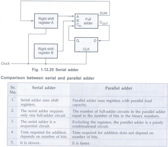
We can implement serial subtractor by replacing full-subtractor instead of full-adder in the Fig. 1.12.25. Here, we will get difference and borrow instead of sum and carry.
Review Questions
1. Design a serial adder using a full adder and a flip flop. AU Dec.-15, Marks 16
2. With diagram explain how two binary numbers are added serially using shift registers. AU: Dec.-19, Marks 6
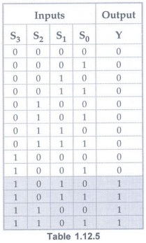
Decimal / BCD Adder
• A BCD adder is a circuit that adds two
BCD digits and produces a sum digit also in BCD.
• To implement BCD adder we require :
• 4-bit binary adder for initial addition
• Logic circuit to detect sum greater
than 9 and
• One more 4-bit adder to add
• The logic circuit to detect sum greater
than 9 can be determined by simplifying the boolean expression of given truth
table.
• Y = 1 indicates sum is greater than 9.
• We can put one more term,
• If any one condition is satisfied we
add 6(0110)in the sum.

• As shown in the Fig. 1.12.26 (b), the
two BCD numbers, together with input carry, are first added in the top 4-bit
binary adder to produce a binary sum.
• When the output carry is equal to zero
(i.e. when sum ≤ 9 and
• When the output carry is equal to one
(i.e. when sum > 9 or
• The output carry generated from the
bottom binary adder can be ignored, since it supplies information already
available at the output-carry terminal.
Example 1.12.4
Design an 8-bit BCD adder using 4-bit binary adder.
Solution:
To implement 8-bit BCD adder we have to cascade two 4-bit BCD adders. In
cascade connection carry output of the lower position (digit) is connected as a
carry input of the higher position (digit). Fig. 1.12.27 shows the block
diagram of 8-bit BCD adder.

Example 1.12.5
Design a BCD to Ex-3 code converter using binary parallel adder.
Solution :

Review Questions
1. Explain with suitable example rules
for BCD addition and design 1-digit BCD adder using IC 74LS83.
2. Draw and explain the basic circuit of
single digit BCD adder using IC 7483. How will you make two digit BCD adder?
Explain the logic of the circuit.
3. What is BCD adder? Design an adder to
perform arithmetic addition of two decimal digits in BCD. AU
Dec.-19, Marks 13
4. How will make 3-digit BCD adder using
4-bit binary adder as a basic building block? Explain with the help of suitable
diagram.
5. Draw and explain 4-bit BCD adder
using IC 7483. Also explain with reference to your design addition of
6. Draw and explain 4-bit BCD adder
using IC 7483. Also explain with example addition of numbers with carry.
BCD Subtractor
Addition of signed BCD numbers can be
performed by using 9's or 10's complement methods. A negative BCD number can be
expressed by taking the 9's or 10's complement. Let us see the implementation
of subtraction process using 9's and 10's complement methods.
Subtractor using 9's Complement Method
The steps for 9's complement BCD
subtraction as follows:
•Find the 9's complement of a negative
number
•Add two numbers using BCD addition
• If carry is generated add carry to the
result otherwise find the 9's complement of the result.
Fig. 1.12.29 shows the logic diagram of
the circuit to implement above mentioned steps to perform BCD subtraction using
9's complement method. As shown in the
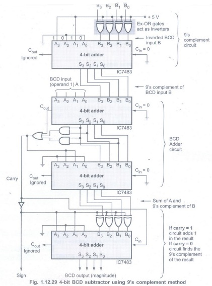
Fig. 1.12.29, first binary adder finds
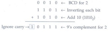
the 9's complement of the negative number. It does this by inverting each bit
of BCD number and adding 10 (1 0 1 02) to it. Let us find the 9's complement of
2
Next two 4-bit binary adders perform the
BCD addition. The last adder finds the 9's complement of the result if carry is
not generated after BCD addition otherwise it adds carry in the result.
Subtractor using 10's Complement Method
The steps for 10's complement BCD
subtraction as follows.
• Find the 10's complement of a negative
number
• Add two numbers using BCD addition
• If carry is not generated find the 10's
complement of the result.
Fig. 1.12.30 shows the logic diagram of
the circuit to implement above mentioned steps to perform BCD subtraction using
10's complement method. As shown in the Fig. 1.12.30, first binary adder finds
the 10's complement of the negative number (9's complement + 1). Next two 4-bit
binary adders perform the BCD addition. Finally, last 4-bit binary adder finds
the 10's complement of the number if carry is not generated after BCD addition.
(See Fig. 1.12.30 on next page)

Review Questions
1. Draw a block diagram of half adder. Write truth table. Draw logic diagram. AU May-06, Marks 2
2. Define full adder. Draw logic circuit and truth table of full adder. AU Dec.-10, Marks 6
3. Implement full adder using two half adders. AU: Dec.-07, May-11, 13, Dec.-12, Marks 8.
4. Draw the schematic of a full adder circuit and give its truth table. AU May-11, Marks 6
5. Design a half-subtractor
combinational circuit to produce the outputs. Difference and borrow. AU:
Dec.-10, May-12, Marks 2
6. Write the logic expressions for the difference and borrow of a half subtractor. AU May-11, Marks 2
7. Write an expression for borrow and difference in a full subtractor circuit. AUMay-10, Marks 2
8. Design full-subtractor circuit and draw necessary truth tables. AU: May-03, May-12, Marks 7
9. What is the drawback in binary parallel adder? How can it be rectified? AU Dec.-07, Marks 3
10. Draw the block diagram of a 2's complement adder/subtractor. AU: May-03, Marks 2
11. Draw the diagram of a 4-bit adder subtractor using full adders. AU: Dec.-12, Marks 4
12. Relate carry generate, carry propagate, sum and carry-out of a carry look ahead adder. AU: Dec.-10, Marks 2
13. Compare the performance of binary serial adder and parallel adders. AU: Dec.-11, Marks 2
14. With a suitable block diagram explain the operation of BCD adder. AU May-09, Dec.-12, Marks 16
15. With neat diagram explain BCD
subtractor using 9's and 10's complement method. AU: Dec.-09, Marks 16
16. Design a combinational circuit that
generates the 9's complement of a BCD digit. AU: Dec.-08, Marks 8
Digital Principles and Computer Organization: Unit I: Combinational Logic : Tag: : Combinational Logic - Digital Principles and Computer Organization - Binary Adder Subtractor
Related Topics
Related Subjects

Digital Principles and Computer Organization
CS3351 3rd Semester CSE Dept | 2021 Regulation | 3rd Semester CSE Dept 2021 Regulation